
Zum Inhalt springen
EPP Europe
  • News
  • Products
  • Applications
  • Technology
  • Semiconductor
  • Inspection
  • Company News
  • Events
EPP Europe
  • Technology
  • Inspection (AOI/AXI)
  • Semiconductor Packaging
  • Company News
  • Products
  • Trade Shows & Events
    EPP Europe Newsletter
    The most important electronics-manufacturing news delivered to your inbox.

    Info

    • Impressum
    • Datenschutz
    • Barrierefreiheit
    • Datenschutzeinstellungen

    Kontakt zur Redaktion

    EPP EuropeKonradin Mediengruppe
    Ernst-Mey-Str. 8, 70771 Leinfelden-Echterdingen

    E-Mail: redaktion@konradin.de
    Folgen Sie uns
    EPP Europe
    © 2026 EPP Europe
    Startseite/Semiconductor-packaging/Artikel
    Upgrade on Warpage Adjustment
    Bildquelle nicht angegeben
    Semiconductor-packaging

    Upgrade on Warpage Adjustment

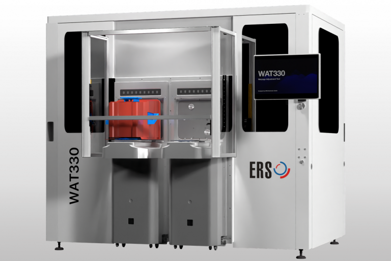
    ERS electronic upgrades its Warpage Adjustment Tool (WAT330), to include powerful capabilities for warpage measurement and correction.
    Veröffentlicht
    20. November 2022
    Lesezeit
    2 Minuten
    Rubrik
    Semiconductor-packaging

    ERS electronic, a leading supplier in thermal management solutions for semiconductor manufacturing, upgrades its Warpage Adjustment Tool (WAT330), to include powerful capabilities for warpage measurement and correction.

    Fan-out Wafer Level Packaging (FoWLP) is one of the most prominent Advanced Packaging technologies. However, wafer deformity, also called “warpage” remains a common issue. As the technology continues to be adopted by OSATs and has transitioned from research to high-volume manufacturing, understanding and handling warpage is crucial to avoid machine downtime and low yield.

    “For FoWLP, one of the major challenges is warpage within the process flow. In our models and tests we observed significant impact from material behavior, layout, geometry and loading history,” says Dr. Olaf Wittler, head of the team Technology Characterization & Reliability Simulation at Fraunhofer IZM. “Therefore, solutions and strategies to control these influence factors for a low warpage are crucial to solve the challenge.”

    ERS has almost 15 years of experience in adjusting warpage of molded wafers in Fan-out. The company is recognized industry-wide for its patented AirCushion technology and TriTemp slide for contactless transport and warpage output of <1 mm. They can both be found in most of ERS’s machines and are typically applied for warpage correction after thermal debonding. However, with the WAT330, companies can address the issue of warpage regardless of where it occurs.

    “Warpage is a top concern in high volume production and will remain so as the structure of FO becomes more complex,” says Debbie-Claire Sanchez, FO Equipment Business Unit manager at ERS electronic. “We therefore extend our warpage correction capabilities to a standalone machine, which can be deployed in-between processes to aid manufacturing.”

    The upgraded WAT330 comes with a HEPA filter system for cleanroom class 100. It is also fully compliant with the GEM300 SEMI standards and compatible with automated product loading and unloading. Another noteworthy upgrade is the machine’s Nitrogen environment, which can reach down to 0.5% O2 level to avoid Cu oxidation. The new WAT330 also features strong vacuum thermal chucks for no-fail wafer handling.


    Mehr aus Semiconductor-packaging

    Weitere aktuelle Artikel aus der Rubrik Semiconductor-packaging.

    Alle Semiconductor-packaging-Artikel
    Nanoscribe Expands Photoresin Portfolio for Micro-Optics Fabrication via Two-Photon PolymerizationFoto: Brecht Corbeel / Unsplash
    Semiconductor-packaging

    Nanoscribe Expands Photoresin Portfolio for Micro-Optics Fabrication via Two-Photon Polymerization

    11. November 2026

    Nanoscribe has detailed its range of photoresins engineered for Two-Photon Polymerization (2PP) and Two-Photon Grayscale Lithography (2GL), targeting high-precision micro-optics manufacturing on silicon, glass, and…

    Canon Launches FPA-6400ES6a KrF Lithography System with 400 Wafers-per-Hour ThroughputFoto: Canon Europe (semicon)
    Semiconductor-packaging

    Canon Launches FPA-6400ES6a KrF Lithography System with 400 Wafers-per-Hour Throughput

    10. November 2026

    Canon has announced the FPA-6400ES6a KrF scanner for semiconductor lithography, combining a throughput of 400 wafers per hour with industry-leading overlay accuracy of 4.0 nm and the ability to handle wafer warpage of…

    Fabmatics absorbs SCI business activities under unified brandFoto: Ludovico Ceroseis / Unsplash
    Semiconductor-packaging

    Fabmatics absorbs SCI business activities under unified brand

    6. November 2026

    Fabmatics has integrated the business activities of SCI under the Fabmatics brand, consolidating the acquired expertise within its semiconductor automation portfolio.

    Entegris and Kioxia Expand Partnership on Materials Innovation for Next-Gen 3D Flash MemoryFoto: Louis Reed / Unsplash
    Semiconductor-packaging

    Entegris and Kioxia Expand Partnership on Materials Innovation for Next-Gen 3D Flash Memory

    6. November 2026

    Entegris and Kioxia are deepening their strategic partnership to co-develop materials and process technologies for future BiCS FLASH 3D NAND architectures, using AI, digital-twin modelling and experimental validation at…

    ← Zurück zu Semiconductor-packagingZur Startseite

