
Dr. Udo E. Frank, Feinfocus
The role played by X-ray systems in the inspection of electronic assemblies is well understood, especially in case of board assemblies densely packed with area-array components. Unlike machine vision and optical inspection equipment, X-ray equipment penetrates materials to expose hidden solder joints and other structures on area-array packages, such as flip chips and BGAs. Once a need for X-ray inspection equipment has been determined, the next question is, which is best for an application: two-dimensional (2D) or three-dimensional (3D) imaging?
For most electronics applications, 2D X-ray systems serve the need, providing a top-down image of the board or package being viewed. More advanced systems also offer the ability to inspect for defects by rotating the part being inspected at oblique angles to the X-ray beam. The target area – the component or interconnect being checked for a defect – can thus be viewed from multiple orientations.
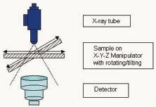
As can be seen in figure 1, the stems consist of: an X-ray source (sealed or open tube), a fixture for holding and manipulating the part being inspected (sample) and the radiation detector. While X-ray tubes are available in various configurations and performance capabilities, ”open” microfocus tubes are used primarily for the high-resolution requirements of electronics assembly and packaging. Such tubes can provide a spatial resolution in the range of 1µm, with geometrical magnifications up to 2400x. An ”open” tube is a stainless steel tube in which a vacuum is continuously created while a ”sealed” tube is generally a tube in which the vacuum is created at the time of manufacture. Sealed tubes, comparatively speaking, do not offer as sharp an image as open tubes. They are also less suitable for high magnification applications because of the larger minimum distance required from the focal spot to the object, and usually have a shorter life due to consumption of the electron gun (filament).
The manipulator is a device for X-, Y-, Z-positioning and rotating/tilting of the sample with high precision. The manipulator should be capable of directional and rotational speeds that can be varied for requirements ranging from quick overview searches at low magnification to very low speeds at high magnification. Such speeds, for X-Y requirements, may be from less than 10µm/sec. to 80mm/sec.
The function of the detector is to process the information of the X-ray image in real-time into an image of visible light that can be observed and assessed by the human eye. While the most common detector is a combination of video camera and image intensifier which converts the X-rays into visible light, other types of detectors recently developed include high-dynamic cameras and flat panel DDDs (direct digital detectors).
The primary advantage of 2D X-ray inspection is the savings in time in viewing an image, as 3D analysis can take twice as long, or even more. The primary limitations of 2D systems become apparent when imaging double-sided boards. In such instances, since X-rays penetrate through components and materials on both sides of a board, the parts on one side can be partially obscured by components on the other side. In the image being viewed, one layer of components can appear to overlay the other. Oblique angle imaging can lessen, and even eliminate, the problem, depending on the X-ray system concept and the complexity of the assembly being inspected.
The most notable advantage of 3D X-ray inspection is the fact that it results in a complete picture of the area of concern. For instance, solder balls on the underside of BGAs, can be viewed from all sides, and defects, such as insufficiently wetted or cracked balls, can be easily identified. The choice between 2D or 3D can be difficult; and the requirement may not always be known until the middle of the inspection procedure, or it may then even change. Actually, an X-ray system that offers both capabilities is likely to be the ideal solution for the majority of applications.
Feinfocus has recently developed the µCT-Fox (figure 2), a combined system that incorporates the following choice: of standard open microfocus tube, or multifocus tube. It enables the operator to select either a microfocus/nanofocus (below 0.3µm feature recognition), or high-power mode, depending on the requirements of the application. The system offers the ability to perform high-resolution 2D inspection for optimum processing speed, while enabling the operator to switch to 3D for inspection of parts and interconnects that cannot be adequately viewed using 2D. Switching from one to the other is accomplished with a keystroke and by viewing a different screen on the same monitor – one screen is for 2D images, while the other is for 3D.
The 3D capability is achieved with a process called axial computed tomography (ACT), employing volume-rendering software. ACT is a reconstruction technology. By taking multiple 2D views and by calculating the volume data (voxels), a 3D image is constructed, such as the transistor shown in figure 3. Typically for 3D inspection, the region of interest (ROI) of the part or interconnect is first located. Then a multitude of images is taken in a 360º circle by rotating the sample, the X-ray beam being projected in a cone, as can be seen in figure 4. The images are subsequently recombined into a 3D visualization model, using the system software.
The manipulator for the 2D/3D X-ray system enables movement around 6 axes in total, the movement being either programmed by CNC (computer numeric control) or controlled with a joystick. The multiple axes thus provide extreme flexibility in positioning the sample for optimum imaging. The high accuracy of the axis allows precise point-to-point measurements in 2D mode. In 3D operation, wall thickness or void volume measurements can be performed directly from the 3D model due to the known size of the voxel (volume element) data.
The combined 2D/3D X-ray inspection system is notable for the ease in which the operator can shift from one mode to the other. Thus, for instance, if a BGA package or another feature is being viewed using the 2D mode and a 3D image is required to examine for a possible defect, the operator simply punches a certain tactile key on the keyboard and begins the 3D operation. As the multiple images are taken in the 360º circle around the part, and the 3D image is constructed by software, the operator begins to view the image on a second screen. Once viewing is completed, the operator can then shift back to 2D and continue the process.
The performance and accuracy of the 2D/3D X-ray system can be attributed to a unique control technology which Feinfocus calls true X-ray intensity (TXI). Unlike systems that attempt to measure and control the input level of the high voltage and current to the X-ray tube, TXI is a process that ensures controlled and stable output intensity for X-ray emission, and consequently a constant focal spot size and spatial position (figure 5.) The result is a sharp and consistent 2D image and data that can be reconstructed into an accurate, viable and complete 3D image. Without precise control over the X-ray intensity, the reconstructed 3D image would be degraded and may not even be possible to achieve.
A combined 2D/3D X-ray system can be used for a variety of applications in a multitude of industries. It is primarily a design, production and quality control tool. For R&D requirements, such equipment can be employed to develop and refine the manufacturing process, and it is ideal for inspecting prototypes of electronic assemblies during pre-production. It can also be used for reverse engineering of existing products. The system is used off-line to inspect components and packages, such as BGAs, flip chips, CSPs (chip scale packages), etc. Cracks, voids, delamination, and other crucial component or package anomalies can be observed and measured in either the 2D or 3D mode, whichever most easily and accurately depicts the defect. The system is particularly useful in the manufacture of sensors and relays, and other MEMS (micro-electro-mechanical) and MOEMS (micro-opto-electro-mechanical) devices.
Röntgeninspektion in der Elektronikfertigung hat in kritischen Applikationen seinen Platz gefunden, speziell dort, wo kein direkter visueller Zugang möglich ist. So kann man einmal das Prüfobjekt insgesamt dsurchstrahlen und einfache Strukturen ohne gegenseitige Überlagerung der Darstellung sicher erkennen, mithin eine 2D-Methode. Oder aber mittels Tomosynthese werden viele aus unterschiedlichen Winkeln aufgenommene Bilder per Software zur einer 3D-komplexen Darstellung zusammengefügt. Bisher waren Anwender von Röntgeninspektionsgeräten immer auf die Entweder-oder-Lösung gestoßen, nun sind beide Verfahren in einem System verfügbar und können je nach Bedarf eingesetzt werden.
L’inspection par rayons X dans la fabrication d’électroniques s’est établie dans les appli-cations critiques, en particulier lorsqu’un accès visuel direct est impossible. Cette technique permet d’une part de visionner l’objet dans son ensemble et de reconnaître les structures simples de manière sûre sans superpositions réciproques, une méthode à deux dimensions donc. Et d’autre part, il est également possible de réunir, à l’aide d’un logiciel, des images prises par tomosynthèse sous différents angles pour obtenir une représentation complexe en trois dimensions. Les utilisateurs d’appareils d’inspection à rayons X devaient jusqu’à présent choisir l’une ou l’autre de ces solutions. Mais les deux procédés sont maintenant réunis au sein d’un même système et peuvent être utilisés au besoin.
La radioscopia ha trovato posto nelle applicazioni più critiche della produzione di componenti elettronici, specialmente dove non è possibile alcun diretto accesso visuale. Infatti, questo procedimento consente di eseguire una sola radioscopia totale dell’oggetto da controllare, di individuare con sicurezza semplici strutture senza alcuna sovrapposizione reciproca delle rappresentazioni, un metodo bidimensionale dunque. Ma anche per mezzo della tomosintesi le immagini riprese da diversi angoli possono essere raggruppate insieme in una rappresentazione tridimensionale molto complessa tramite l’applicazione di uno speciale software. Finora gli utenti di apparecchi per radioscopia si sono ripetutamente trovati davanti alla soluzione ”o la va o la spacca”, mentre adesso ambedue i procedimenti sono disponibili in un solo sistema e possono essere applicati secondo le esigenze individuali.



