
Christoph Scheiring, Datacon/Austria
There is a strong trend toward converting the potential of ultra-thin silicon chips into innovative products which are thinner, even higher integrated and more cost-effective. This involves special design methods which lead to flexible and paper-thin packages such as smart cards and labels. Thin chips can also be stacked very easily, which, together with the multi-chip module technology, results in very flat packages for memory modules and entire systems. Finally, thin chips with their low electrical resistance ensure reduced power dissipation, thus lowering operating temperature and increasing reliability – which is especially valuable for power electronics.
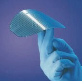
The thickness of semiconductor chips is set to decrease by well over half in the immediate future: in power electronics from at the moment approximately 250µm to between 120 and 60µm only. For smart-card or smart-label applications with their current 120 to 150µm, values below 50µm are being targeted, above all for so-called “smart paper” (figure 1).
Cost-effective, high-volume manufacturing of such extremely flat, miniaturized components requires suitable production gear for the bonding of ultra-thin chips. The industry is currently working intensively on further development, because the availability of automation equipment for the processing of ultra-thin wafers and chips is the key requirement for a extensive range of possible applications, such as identification systems, power electronics, mobile communication, computers, domestic appliances and medical electronics.
Two very important prerequisites for success in this market segment are an extendable, high-precision equipment basis and experience with these upcoming technologies. The latter is important because ultra-thin silicon is highly fragile and can easily be damaged during handling. Suitable machines for processing ultra-thin wafers must therefore have industry-standard techniques for smooth handling and gentle processing as well as secure transport. The following are especially important: a flexible machine platform, automated wafer handling, combined flip-chip and die-attach capabilities, automated tool changing, different techniques for epoxy application, gentle and synchronous ejection of chips, capabilities for substrate and chip heating, and special tools.
Against the background of typical industrial applications, Datacon began a strategic research project for innovative, extremely flat packaging solutions several years ago, which it is hoped will lead to suitable machines. As a result, a prototype for bonding ultra-thin chips has been engineered. The machine is based on the 2200 apm model as part of the European IST project Flex-Si (ultra-thin packaging solutions using thin silicon), which formed a very good basis for further development in this field (figure 2).
The performance characteristics of this equipment, which is optimized for the handling of ultra-thin chips, include the following features: synchronous ejection and gentle chip transfer, adjustment of needle ejection system and tool to the chip geometry, special tools, ejection at intervals, programmable low-speed transport paths, precisely defined bond forces with high-precision repetition, and Z-axis control for bonding and epoxy application. Particularly noteworthy is the synchronous sequence of motions of the pick-up tool and the ejector needles, whereby the detachment of the chip from the backing material is supported by vacuum (figure 3).
Now that the feasibility of handling ultra-thin wafers with the modified 2200 apm flip-chip bonder has been confirmed, the next step is to establish the performance capability of the machine under various simulated production conditions, develop it further and finally evaluate it. Datacon as part of the current will perform this step. EU project FLIBUSI (flip-chip die bonder for ultra-thin silicon). For this project,two modules are being used which of-fer characteristic values with respect to performance and functionality in practi-cal operation, and each achieve a throughput of 2000 to 3000 components per hour (cph).
Each module has a bond head for picking up and positioning the chips, which can execute highly precise movements in four degrees of freedom (X, Y, Z, F or phi respectively). A transport unit moves the substrate from the input stage to the bonding area and onward to the output system. The wafers are taken from magazine and transported to the wafer platform, where an ejection system detaches the individual chips from the backing film. The flip unit takes over the detached chip and rotates it by 180º. The chip is then passed to the bond head, which moves it as necessary to have the epoxy or soldering flux applied via the dipping station, and then to the final bonding position on the substrate.
The particular strength of this piece of equipment lies in its flexibility in handling different thin silicon materials and the high precision of its individual processes while maintaining a good throughput. There are special functions for adjusting the handling mechanisms (ejection system, flip unit, bond head) and reducing the damage possible to thin chips and ensure fast flip-chip cycles of very small chips on substrates with a large surface area of 200 to 250mm.
To help promote the use of ultra-thin silicon through automated industrial equipment for flip-chip positioning on sub-strates, Datacon is working with several partners: The equipment is located at the Fraunhofer Institute for Silicon Technology (ISIT) in Itzehoe, Germany, where the evaluation also takes place. Two users, Pav Card and Danfoss Silicon Power, contribute sample applications from very different fields. A smart-label product from Pav Card is being tested: the chipsize is approximately 1mm2 with a thick-ness of less than 50µm. A power-electronics component with a larger surface area of 100 mm2 and a thickness of 100µmhas been provided by Danfoss. Both com-panies are actively involved in evaluating the device under simulated production conditions.
As part of the project, various performance characteristics of the flip-chip bonder for ultra-thin silicon will be tested under simulated production conditions until the beginning of 2003. Among these features are: process quality, yield, MTBF (mean time to maintenance), MTTR (mean time to repair), effective usage time, throughput and total costs. The equipment will also be compared with com-petitor’s offers. As revealed by a survey from Semiconductor Business News, European device outfitters have succeeded in significantly increasing the satisfaction of their customers. Further developments will ensure that this also applies in thefuture.
Within the context of the EU project FLIBUSI (flip-chip die bonder for ultra-thin silicon) as part of the SEA (semiconductor equipment assessment) program, the use of the Datacon 2200 apm flip-chip die bonder with ultra-thin chips was tested, developed further and finally evaluated from the following aspects:
• Chip pick-up from the wafer feed (detachment from backing film)
• Influence of different backing materials (blue tape, UV tape, thermally supported detachment) on ejection
• Positioning speed and accuracy of the flip-chip process
• Use in production of smart labels with flip-chip assembly of ultra-thin chips (50µm) on flexible substrates
• Use in production of power modules with bonding on copper-bonded substrates (100µm)
• Evaluation of machine performance characteristics under different conditions
• Cost-effectiveness for the bonding of ultra-thin chips
• Benchmark compared with competitor products
The status and the evaluation results can be viewed at
Noch liegen übliche Waferdicken bei circa 250 µm, aber schon sind 100 bis 50 µm angepeilt und auch bald im industriellen Maßstab realisierbar, vorausgesetzt das Equipment kann die dünnen und zerbrechlichen Scheiben adäquat handeln. Die papierdünnen und flexiblen Chips, die solcherart dann herstellbar sind, eröffnen für Halbleiter bisher nicht mögliche Anwendungsfelder mit hohem Potential. Für ein EU-Projekt wurde ein Die-Bonder entwickelt, der hohen Handling-Anforderungen entspricht.
Si les épaisseurs usuelles des tranches de silicium sont encore de l’ordre de 250 µm, on vise à atteindre les 100 à 50 µm, chose réalisable à brève échéance à l’échelle industrielle à condition que l’équipement soit capable de manipuler comme il se doit ces fragiles tranches. Souples et fins comme une feuille de papier, les chips ainsi obtenus ouvrent aux semi-conducteurs de nouvelles applications à haut potentiel. Un Die-Bonder qui satisfait à de sévères exigences en matière de manipulation a été développé pour un projet européen.
Attualmente gli abituali spessori wafer corrispondono ancora a circa 250 µm, ma si stanno già localizzando misure da 100 fino a 50 µm, che saranno prossimamente realizzabili anche a livello industriale, fatta salva la premessa, che l’equipaggiamento sia comunque in grado di trattare in maniera adeguata le fragilissime lastre. I chip flessibili e sottili come la carta, che potranno poi essere prodotti in questo modo, per i semiconduttori non costituiscono alcuni errori d’applicazione finora possibili ad elevato potenziale. Per un progetto UE è stato sviluppato un Die-Bonder, corrispondente ad elevate aspettative di handling.



