
Zum Inhalt springen
EPP Europe
  • News
  • Products
  • Applications
  • Technology
  • Semiconductor
  • Inspection
  • Company News
  • Events
EPP Europe
  • Technology
  • Inspection (AOI/AXI)
  • Semiconductor Packaging
  • Company News
  • Products
  • Trade Shows & Events
    EPP Europe Newsletter
    The most important electronics-manufacturing news delivered to your inbox.

    Info

    • Impressum
    • Datenschutz
    • Barrierefreiheit
    • Datenschutzeinstellungen

    Kontakt zur Redaktion

    EPP EuropeKonradin Mediengruppe
    Ernst-Mey-Str. 8, 70771 Leinfelden-Echterdingen

    E-Mail: redaktion@konradin.de
    Folgen Sie uns
    EPP Europe
    © 2026 EPP Europe
    Startseite/Semiconductor-packaging/Artikel
    Strong momentum pushed by the giants
    Bildquelle nicht angegeben
    Semiconductor-packaging

    Strong momentum pushed by the giants

    The top 8 advanced packaging players dominate the market and continue with heavy investment. • The advanced packaging industry is expected to have a 9.6%
    Veröffentlicht
    12. September 2022
    Lesezeit
    2 Minuten
    Rubrik
    Semiconductor-packaging

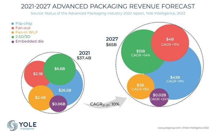
    • The advanced packaging industry is expected to have a 9.6% CAGR (Compound Annual Growth Rate) between 2021 and 2027 to $65 billion.
    • The advanced packaging segment as compared with traditional packaging market continues to increase, with more than 50% of the market by 2027.
    • The highest advanced packaging market share belongs to the Flip-Chip platform, with 70% of the market in 2021. The highest CAGR is expected from ED , 2.5D/3D, and fan-out at 24%, 14%, and 11%, respectively.

    Six players, including 2 IDMs (Intel and Samsung), a foundry (TSMC), and the top 3 global OSATs (ASE, Amkor, JCET), process over 80% of advanced packaging wafers. OSATs accounted for 65% of the advanced packaging wafers in 2021. Foundries are taking advanced packaging business from OSATs with 14% and IDMs with 21%.

    IC substrate and PCB manufacturers, including SEMCO, Unimicron, AT&S, and Shinko, are entering the advanced packaging arena. They offer panel-level fan-out packages and embedded dies (and passives) in organic substrates in response to the accelerated adoption of fan-out packaging. These players are taking advantage of their substrate manufacturing know-how, panel line and equipment availability, and thin RDL technology development.

    On the other hand, OSATs are expanding their testing expertise, while traditional pure test players are investing in packaging & assembly capabilities. Top OSATs are investing in IC testing capacity to capture the test market, and pure test houses, such as KYEC and Sigurd Microelectronics, are adding packaging/assembly capabilities in their service offering through M&As or investing in R&D.

    Overall, there is a paradigm shift in the packaging / assembly business, traditionally the domain of OSATs & IDMs. Players from different business models, foundries, substrate/PCB suppliers, and EMS/ODMs are entering packaging & assembly, cannibalizing the OSAT business.

    Substrates have been in tight supply due to strong demand for high-end CPUs, GPUs, and 5G networking chips by major chipmakers. The COVID-19 pandemic, high inflation, and geopolitical tensions are continuing to negatively impact material supplies. The delivery lead time of ABF substrates has been extended to nearly three quarters from 4-5 months due to demand growth outpacing capacity expansion, and prices have risen from 15% to 25%.


    Mehr aus Semiconductor-packaging

    Weitere aktuelle Artikel aus der Rubrik Semiconductor-packaging.

    Alle Semiconductor-packaging-Artikel
    Nanoscribe Expands Photoresin Portfolio for Micro-Optics Fabrication via Two-Photon PolymerizationFoto: Brecht Corbeel / Unsplash
    Semiconductor-packaging

    Nanoscribe Expands Photoresin Portfolio for Micro-Optics Fabrication via Two-Photon Polymerization

    11. November 2026

    Nanoscribe has detailed its range of photoresins engineered for Two-Photon Polymerization (2PP) and Two-Photon Grayscale Lithography (2GL), targeting high-precision micro-optics manufacturing on silicon, glass, and…

    Canon Launches FPA-6400ES6a KrF Lithography System with 400 Wafers-per-Hour ThroughputFoto: Canon Europe (semicon)
    Semiconductor-packaging

    Canon Launches FPA-6400ES6a KrF Lithography System with 400 Wafers-per-Hour Throughput

    10. November 2026

    Canon has announced the FPA-6400ES6a KrF scanner for semiconductor lithography, combining a throughput of 400 wafers per hour with industry-leading overlay accuracy of 4.0 nm and the ability to handle wafer warpage of…

    Fabmatics absorbs SCI business activities under unified brandFoto: Ludovico Ceroseis / Unsplash
    Semiconductor-packaging

    Fabmatics absorbs SCI business activities under unified brand

    6. November 2026

    Fabmatics has integrated the business activities of SCI under the Fabmatics brand, consolidating the acquired expertise within its semiconductor automation portfolio.

    Entegris and Kioxia Expand Partnership on Materials Innovation for Next-Gen 3D Flash MemoryFoto: Louis Reed / Unsplash
    Semiconductor-packaging

    Entegris and Kioxia Expand Partnership on Materials Innovation for Next-Gen 3D Flash Memory

    6. November 2026

    Entegris and Kioxia are deepening their strategic partnership to co-develop materials and process technologies for future BiCS FLASH 3D NAND architectures, using AI, digital-twin modelling and experimental validation at…

    ← Zurück zu Semiconductor-packagingZur Startseite

