
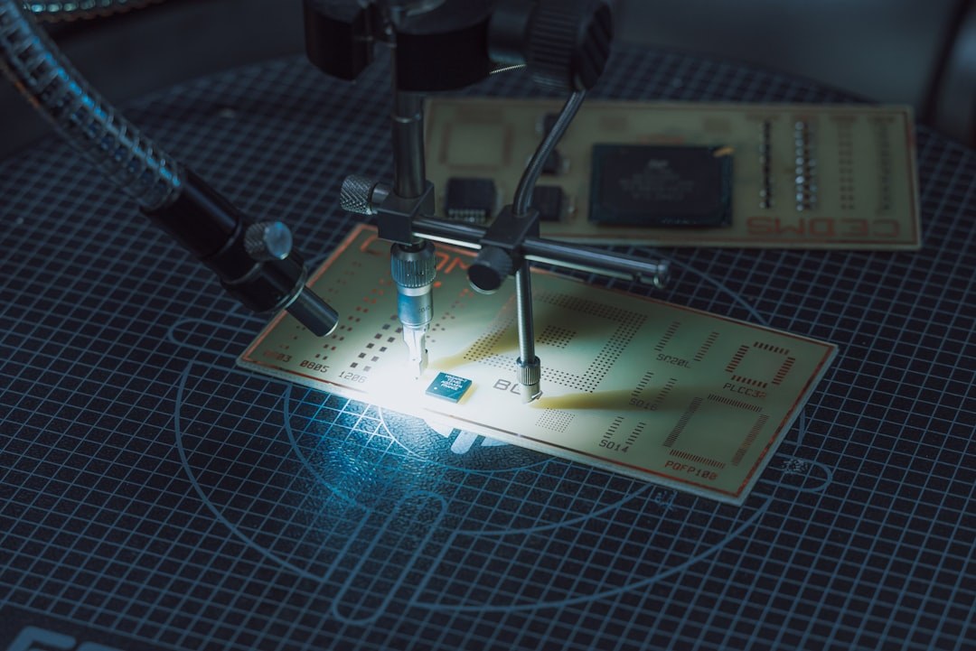
In surface mount technology, the deposition of solder paste onto a printed circuit board represents the starting point of the entire assembly chain. Studies consistently attribute between 60 and 70 percent of all soldering defects in SMT production to errors that originate in this single step — before a single component has been placed and before the board has entered the reflow oven. Despite its apparent simplicity, stencil printing is a highly complex process governed by the interaction of numerous mechanical, material-related and environmental variables. Understanding these variables and controlling them systematically is therefore a prerequisite for any electronics manufacturer aiming at reliable, repeatable results.
The core task of stencil printing is to transfer a precisely defined volume of solder paste through apertures in a thin metal foil — the stencil — onto the land pads of a bare or pre-assembled PCB. The paste volume deposited on each pad determines the quality of the subsequent solder joint after reflow. Too little paste leads to insufficient wetting, open joints or component tombstoning; too much paste promotes bridging, balling and voiding. Achieving the correct volume consistently across all pads on a board, from the first print of a shift to the last, is the central challenge of the process.
The Stencil: Foil Material, Fabrication and Aperture Design
Modern stencils are almost universally produced from stainless steel foil, typically in thicknesses ranging from 80 to 200 µm, with 120 to 150 µm representing the most common range for standard mixed-technology assemblies. The fabrication method has a decisive influence on the wall quality of the apertures: laser-cut stencils offer high flexibility and are the industry standard, while electroformed nickel stencils provide exceptionally smooth aperture walls and are preferred for ultra-fine-pitch applications. Electropolishing or nano-coating of laser-cut stencils bridges the gap between the two, improving paste release from aperture walls without the cost of full electroforming.
Aperture design is governed primarily by two geometric ratios. The area ratio — the aperture opening area divided by the aperture wall area — should exceed 0.66 as a general rule of thumb to ensure reliable paste release. For square or circular apertures this translates directly into a minimum side-to-stencil-thickness ratio. The aspect ratio (aperture width divided by stencil thickness) should remain above 1.5. When these ratios fall below the recommended thresholds, paste cohesion to the walls exceeds the force driving paste onto the pad, resulting in inconsistent transfer efficiency. Step stencils, which incorporate locally thinned or thickened regions, address the competing paste volume requirements of mixed-component boards that carry both fine-pitch ICs and large connectors or power devices on the same substrate.
Solder Paste Rheology and Its Role in Print Quality
Solder paste is a complex, non-Newtonian fluid — specifically a thixotropic material whose viscosity decreases under shear stress and recovers at rest. This behaviour is essential for the printing process: the paste must flow readily under squeegee pressure to fill apertures completely, yet retain sufficient body after printing to hold its shape until reflow. Paste viscosity is characterised in the laboratory using viscometers operating at defined shear rates, but practical print performance depends on a broader set of rheological properties including slump resistance, tack and tackiness retention over time.
The particle size distribution of the alloy powder within the paste is classified by the IPC J-STD-005 and the more recent IPC J-STD-005A standards into type designations (Type 3, Type 4, Type 4.5, Type 5 and finer). Finer powder types are required for stencil apertures serving component pitches below 0.4 mm, as a general guideline recommends that the minimum aperture dimension should be at least five times the maximum particle diameter. Alloy composition — most commonly Sn-Ag-Cu (SAC) in its various ratios for lead-free production — affects not only the melting point and mechanical properties of the final joint but also the print behaviour of the paste, since alloy density influences powder settling and slump characteristics.
Key Process Parameters: Squeegee, Speed, Pressure and Separation
The squeegee is the mechanical element that drives paste across the stencil surface and forces it into the apertures. Metal squeegee blades — typically hardened stainless steel — have largely replaced polyurethane in high-precision production because they maintain a consistent attack angle and do not flex under pressure in a way that would scoop paste out of apertures after filling. Squeegee speed is one of the primary process levers: lower speeds allow more time for paste to roll and fill apertures by hydrodynamic pressure, while higher speeds increase throughput but risk incomplete fill, particularly in small or high-aspect-ratio apertures.
Squeegee pressure must be set to achieve clean wiping of the stencil surface without pressing so hard that paste is extruded from already-filled apertures or that the blade deflects. Excessive pressure accelerates stencil wear and can damage the foil surface coating. Snap-off distance — the gap between the bottom of the stencil and the PCB surface during printing — has been largely replaced in modern printers by contact printing with controlled separation speed. The z-axis separation speed after printing critically affects paste release: a slow, controlled lift allows the paste column to shear cleanly at the pad surface rather than being pulled out of the aperture, particularly important for fine-pitch apertures.
Solder Paste Inspection: Closing the Loop with SPI
Solder paste inspection (SPI) systems, positioned immediately after the printer in the SMT line, use structured light projection, laser triangulation or fringe projection to generate three-dimensional height maps of every printed paste deposit on the board. From these measurements the system calculates deposit volume, area coverage, height, offset from the pad centre and shape regularity for each individual pad. Because SPI delivers 100 percent inspection of every deposit on every board in production time, it provides the statistical basis for closed-loop process control — feeding correction data back to the printer to compensate for systematic drift before defective boards accumulate.
Modern SPI platforms report volume transfer efficiency (VTE) — the ratio of measured paste volume to the theoretical aperture volume — as the primary quality metric, since it normalises measurements across pads of different sizes and allows direct comparison of print performance for components ranging from 01005 chip resistors to QFN ground paddles. Capability indices such as Cpk, calculated from SPI measurement data, enable the production engineer to quantify process stability over time and to identify whether variation originates from paste rheology changes, stencil wear, board support issues or printer mechanics.
Environmental Controls and Practical Process Management
Temperature and relative humidity in the print environment exert a measurable influence on paste viscosity and open time — the period during which the paste on the stencil remains printable. Most paste manufacturers specify an operating window of 20 to 25 °C and 40 to 60 percent relative humidity. Deviation from these conditions, particularly elevated temperature combined with low humidity, accelerates solvent evaporation and flux oxidation in the paste bead, leading to viscosity increase, graining and ultimately poor print quality. Climate control in the SMT print area is therefore not a luxury but a process requirement.
Stencil cleaning — both automatic underside wiping integrated into the printer and periodic full manual cleaning — removes paste residues from the stencil underside and from within apertures that would otherwise cause smearing and bridging in subsequent prints. The frequency of automatic wipe cycles is itself a process parameter that must be optimised: too infrequent and paste bleeds under the stencil; too frequent and throughput is reduced unnecessarily. Advanced printers allow condition-based wipe triggering based on inspection feedback rather than fixed cycle intervals. With the growing integration of print process data into manufacturing execution systems (MES), real-time trending of SPI data against environmental sensor readings and printer parameter logs is becoming standard practice in high-reliability electronics manufacturing, forming a solid foundation for data-driven process optimisation.