
Zum Inhalt springen
EPP Europe
  • News
  • Products
  • Applications
  • Technology
  • Semiconductor
  • Inspection
  • Company News
  • Events
EPP Europe
  • Technology
  • Inspection (AOI/AXI)
  • Semiconductor Packaging
  • Company News
  • Products
  • Trade Shows & Events
    EPP Europe Newsletter
    The most important electronics-manufacturing news delivered to your inbox.

    Info

    • Impressum
    • Datenschutz
    • Barrierefreiheit
    • Datenschutzeinstellungen

    Kontakt zur Redaktion

    EPP EuropeKonradin Mediengruppe
    Ernst-Mey-Str. 8, 70771 Leinfelden-Echterdingen

    E-Mail: redaktion@konradin.de
    Folgen Sie uns
    EPP Europe
    © 2026 EPP Europe
    Startseite/News/Artikel
    Solutions to reduce CO2 for advanced node lithography lithography & etch
    Bildquelle nicht angegeben
    News

    Solutions to reduce CO2 for advanced node lithography lithography & etch

    Imec, a research and innovation hub in nanoelectronics and digital technologies, has presented an overview of advanced node lithography and etch related
    Veröffentlicht
    18. März 2024
    Lesezeit
    2 Minuten
    Rubrik
    News

    Semiconductor devices fabricated in 2021 had a CO2 equivalent footprint of about 175 megatonnes, equivalent to the yearly emissions associated with about 30 million people. Using imec.netzero, a virtual fab model developed in the frame of imec’s Sustainable Semiconductor Technologies and Systems (SSTS) program, the organization showed that together, lithography and etch contribute over 40% of advanced logic node Scope 1 and Scope 2 emissions.

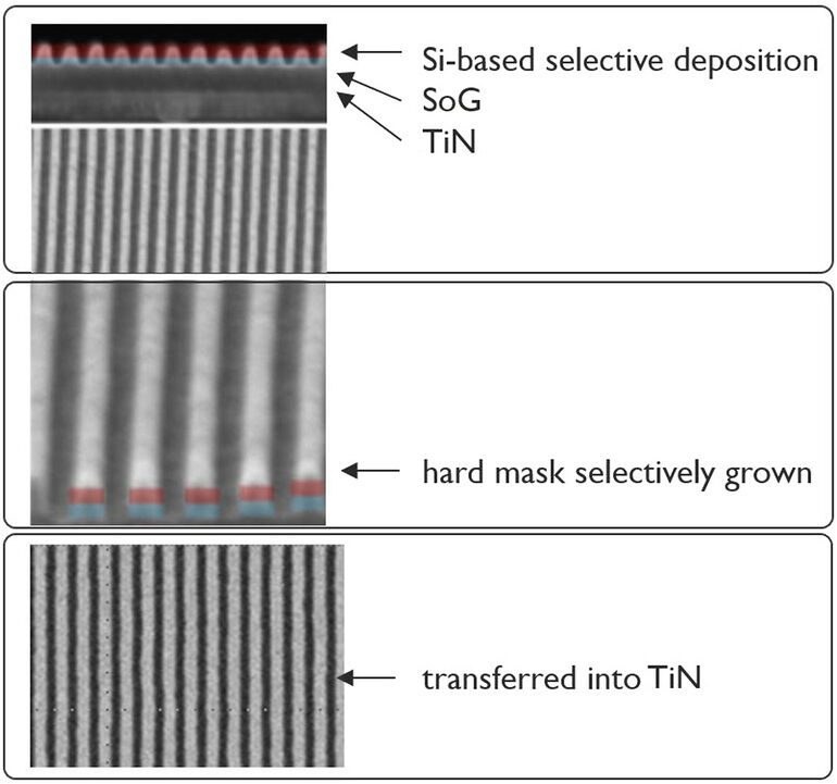
    “There are important levers available to reduce that impact,” said Emily Gallagher, a principal member of the technical staff at imec. “For example, most dry etch processes rely on fluorinated compounds that have very high global warming impact, and direct emissions associated with those processes are high. To minimize their consumption and thus reduce their impact, we present process and design directions for future patterning enabling ultra-thin resists and underlayers, minimal passivation and low process temperatures for etch. Using these principles, we demonstrated a High-NA-compatible metal line etch process step that has ~6% of the process gas emissions relative to the reference process before abatement.”

    For lithography, the larger challenge are the emissions associated with generating electricity. Consequently, the levers are using greener energy, reducing the number of multi-patterning steps, reducing photoresist dose, and enhancing scanner throughput. “If an EUV scanner’s throughput is reduced by 20% and the impact is modeled with imec.netzero through the full process of an advanced logic node wafer, we achieve over 6% more Scope 2 emissions (energy component),” said Gallagher. “In addition, replacing one EUV low-NA litho-etch-litho-etch (LELE) via process module with the High-NA EUV single exposure equivalent can reduce emissions by about 30%; this reduction is achieved by eliminating process steps and despite the increase in power consumption associated with the High-NA scanner’s advanced stages and drive laser.

    “Sustainability is important for imec and we are pleased to see that it is also gaining importance at the SPIE Advanced Lithography and Patterning conference. An informal search of papers shows a promising trend: in 2018 there was only one paper that mentioned sustainability and now, only six years later, the conference is anticipating 45 papers in the sustainability track … Last year shattered global climate records, so it is essential that we all take action as organizations and as individuals. Imec has embraced this action at all levels including our research.”


    Mehr aus News

    Weitere aktuelle Artikel aus der Rubrik News.

    Alle News-Artikel
    Microtronic Takes on Distribution of iRaptor EYE Thermal Profiler in GermanyFoto: Laurens van der Drift / Unsplash
    News

    Microtronic Takes on Distribution of iRaptor EYE Thermal Profiler in Germany

    9. November 2026

    German distributor Microtronic has announced it will represent iRaptor LDA and its EYE thermal profiler in Germany. The Portuguese developer's system extends beyond conventional 2D time-temperature profiling by…

    Indium Corporation Presents Solder Materials Research at SMTAI 2026Foto: Indium Corporation
    News

    Indium Corporation Presents Solder Materials Research at SMTAI 2026

    29. Oktober 2026

    Indium Corporation is fielding five specialists at SMTA International 2026 to present new findings on solder paste rheology, BGA ball alloy selection for lower-temperature reflow, and the effect of print gap on paste…

    KYZEN to Present AQUANOX Aqueous Cleaning Chemistries at SMTA International 2026Foto: Vishnu Mohanan / Unsplash
    News

    KYZEN to Present AQUANOX Aqueous Cleaning Chemistries at SMTA International 2026

    16. Oktober 2026

    KYZEN will exhibit its AQUANOX line of aqueous electronics cleaning chemistries at SMTA International, October 27–29, 2026, highlighting prolonged bath life as a process efficiency and cost-reduction lever for…

    Fuji America and Cybord Partner to Integrate Visual AI Component Inspection into SMT LinesFoto: Cybord
    News

    Fuji America and Cybord Partner to Integrate Visual AI Component Inspection into SMT Lines

    29. August 2026

    Fuji America Corporation and Cybord have announced a strategic partnership to embed AI-powered component analytics directly into SMT production lines, enabling 100% real-time inspection of electronic components during…

    ← Zurück zu NewsZur Startseite

