
Zum Inhalt springen
EPP Europe
  • News
  • Products
  • Applications
  • Technology
  • Semiconductor
  • Inspection
  • Company News
  • Events
EPP Europe
  • Technology
  • Inspection (AOI/AXI)
  • Semiconductor Packaging
  • Company News
  • Products
  • Trade Shows & Events
    EPP Europe Newsletter
    The most important electronics-manufacturing news delivered to your inbox.

    Info

    • Impressum
    • Datenschutz
    • Barrierefreiheit
    • Datenschutzeinstellungen

    Kontakt zur Redaktion

    EPP EuropeKonradin Mediengruppe
    Ernst-Mey-Str. 8, 70771 Leinfelden-Echterdingen

    E-Mail: redaktion@konradin.de
    Folgen Sie uns
    EPP Europe
    © 2026 EPP Europe
    Startseite/Productronica-2017/Artikel
    Solder Paste Inspection: The Critical Gateway to First-Pass Yield in SMT Assembly
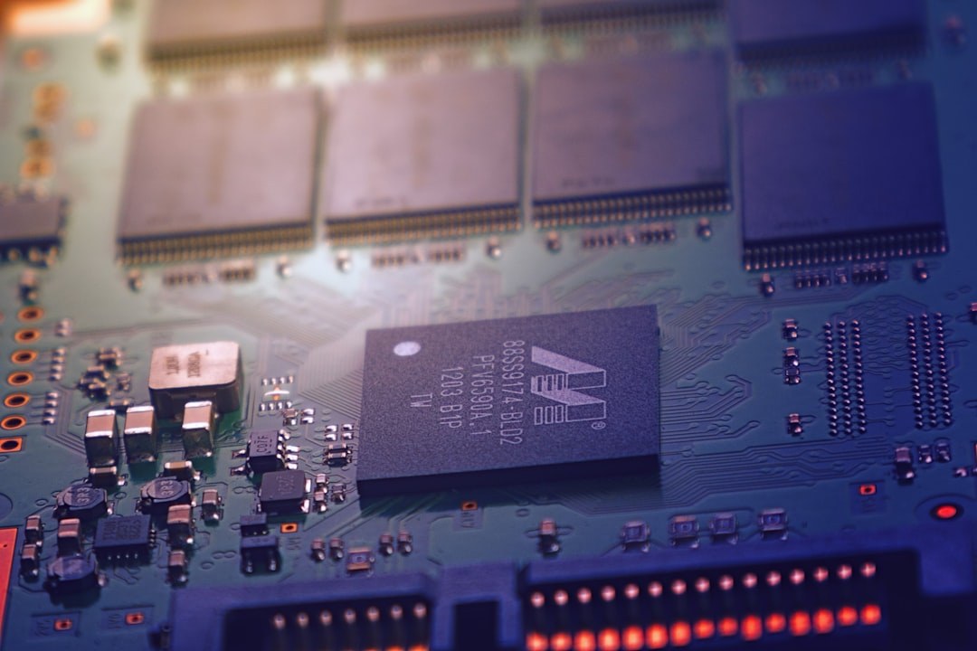
    Foto: Johannes Plenio / Unsplash
    Productronica-2017

    Solder Paste Inspection: The Critical Gateway to First-Pass Yield in SMT Assembly

    Fundamentals of SPI Technology
    Veröffentlicht
    14. November 2026
    Lesezeit
    6 Minuten
    Rubrik
    Productronica-2017

    In surface-mount technology assembly, the stencil printing process is statistically responsible for approximately 60 to 70 percent of all downstream soldering defects. Insufficient paste volume, misregistration, bridging and skipped deposits are root causes that propagate invisibly through reflow and only manifest as measurable faults during automated optical inspection or functional test — at a point where rework costs are significantly higher. Solder paste inspection, commonly abbreviated as SPI, addresses this problem by measuring the printed paste deposit immediately after the stencil printer and before component placement, closing a feedback loop that classical 2D optical inspection could never provide.

    The concept of in-line SPI is not new, but the precision, throughput and actionable data output of modern 3D SPI systems have transformed it from a supplementary check into a mandatory process control element on competitive SMT lines. The following overview explains the underlying measurement physics, the key metrics evaluated, integration into the production line and the requirements that determine system selection.

    Measurement Principles: From 2D Optical to Structured-Light 3D

    Early SPI systems operated exclusively in two dimensions, capturing top-down greyscale or colour images of the printed board to assess paste area and registration offset. While computationally simple and fast, 2D SPI cannot determine paste height or volumetric fill, leaving the most critical parameters unmeasured. A paste deposit that appears correctly shaped in plan view may still be insufficiently tall, entrapping a void or exhibiting a collapsed profile that will cause a solder joint defect after reflow.

    Contemporary 3D SPI systems rely predominantly on structured-light triangulation, also referred to as phase-shift moiré or fringe projection. A projector casts a series of sinusoidal stripe patterns onto the board surface at a defined angle; one or more cameras, positioned at a known offset, capture the resulting fringe images. Local height at every pixel is computed from the phase shift of the observed fringe relative to the projected reference. By acquiring multiple phase-shifted fringe sets and applying phase-unwrapping algorithms, the system resolves absolute height across the full field of view with sub-micrometre repeatability under controlled conditions. Some platforms combine fringe projection with colour imaging in a single pass, acquiring both volumetric and 2D texture data simultaneously to maintain line throughput.

    Key Metrics and Acceptance Criteria

    The primary measurement outputs of a 3D SPI system are paste height, paste area and calculated paste volume for each individual deposit. Volume is considered the most robust indicator of print quality because it integrates height distribution across the entire deposit footprint and is least sensitive to minor shape irregularities. The measured volume is compared against the theoretical aperture volume derived from the stencil design — typically expressed as a percentage. Industry practice, guided by IPC-7711 and process capability studies at leading EMS providers, commonly defines acceptance windows in the range of 50 to 150 percent of nominal volume, though tighter windows down to 70 to 130 percent are applied for fine-pitch and area-array components.

    ← Zurück zu Productronica-2017Zur Startseite

    Beyond volumetric metrics, SPI systems evaluate positional offset in X and Y relative to the pad centroid, shape regularity, presence of bridging between adjacent deposits, and coplanarity of the board surface as an indicator of support pin placement. Height uniformity across the board — particularly the difference between corner and centre deposits — provides a direct diagnostic of squeegee pressure distribution and stencil release behaviour.

    Closed-Loop Feedback and Process Control Integration

    The strategic value of SPI extends well beyond pass/fail sorting. When SPI data is fed back automatically to the upstream stencil printer via a standardised communication interface, the assembly line can self-correct print parameters such as squeegee speed, print pressure and separation speed without operator intervention. This closed-loop configuration is sometimes described as automatic print optimisation or print-to-SPI feedback control. The effectiveness of such a loop depends on the statistical robustness of the SPI measurement — a system with high measurement uncertainty will generate false corrections that destabilise the process rather than improve it.

    For traceability and statistical process control purposes, SPI systems export per-deposit measurement data to MES platforms or dedicated SPC software. Trend monitoring of Cpk values across a production lot allows process engineers to detect stencil wear, paste rheology drift caused by environmental changes in humidity or temperature, and printer mechanical degradation before defect rates increase. This data-driven approach aligns directly with the requirements of smart factory concepts and IPC-CFX (Connected Factory Exchange), the emerging open communication standard for SMT equipment interoperability.

    Stencil and Paste Material Interactions

    SPI results cannot be interpreted in isolation from the upstream consumables that determine paste deposition. Stencil aperture design — specifically the area ratio, defined as the aperture area divided by the sidewall area — governs paste release efficiency. An area ratio below 0.66 is widely regarded as the threshold below which consistent paste release becomes unreliable with standard laser-cut stainless steel stencils. Nano-coating or electroform stencil technologies can extend printability to lower area ratios, but SPI data provides the empirical evidence needed to validate such claims on a given paste-stencil-board combination.

    Solder paste rheology directly influences the measurement. High-metal-content, fine-powder pastes — Type 4 and Type 5 powders as defined by IPC J-STD-005 — exhibit different slump characteristics after printing compared to coarser Type 3 pastes. Because slump occurs within seconds to minutes after print, the timing between print completion and SPI measurement affects the apparent deposit geometry. Best practice is to minimise this interval and maintain consistent timing across all boards in a production run to ensure comparable SPI data.

    System Selection Criteria and Practical Implementation

    When evaluating SPI equipment, the technical parameters that require close scrutiny include measurement repeatability and reproducibility expressed as a gauge R&R percentage, field of view relative to maximum board size, cycle time at rated resolution, and the minimum detectable feature size relevant to the smallest apertures in the production mix. For high-volume consumer electronics lines processing boards with 0201 and 01005 components, measurement resolution in the lateral plane must be sufficient to resolve deposits below 300 micrometres in diameter without ambiguity.

    Physical integration into the SMT line requires consideration of conveyor width range, board weight capacity, edge-belt or centre-support transport mode, and compatibility with smeared-paste boards that may need to pass through without contaminating the transport system. Ergonomic factors including programming effort for new board types, the intuitiveness of the recipe editor and the clarity of the graphical defect reporting interface determine the practical adoption rate among operators and process engineers on the production floor.

    Outlook: SPI as the Foundation of Predictive Quality Management

    As component miniaturisation continues with 008004 passives entering volume production and heterogeneous assembly combining standard SMT with embedded components and advanced packaging, the demands placed on solder paste inspection will intensify. Future SPI development focuses on higher lateral resolution, faster multi-field acquisition through parallel camera architectures, and deeper integration with machine learning algorithms capable of correlating SPI signatures with reflow outcome data collected by downstream AOI and AXI systems.

    The fundamental principle, however, remains unchanged: measuring and controlling the solder paste deposit before component placement is the most cost-effective intervention point in the entire SMT process chain. Manufacturers who treat SPI as an optional line element rather than a mandatory process control node accept a structural disadvantage in yield, rework cost and customer return rates that becomes increasingly difficult to absorb as product complexity and customer quality expectations continue to rise.