
Zum Inhalt springen
EPP Europe
  • News
  • Products
  • Applications
  • Technology
  • Semiconductor
  • Inspection
  • Company News
  • Events
EPP Europe
  • Technology
  • Inspection (AOI/AXI)
  • Semiconductor Packaging
  • Company News
  • Products
  • Trade Shows & Events
    EPP Europe Newsletter
    The most important electronics-manufacturing news delivered to your inbox.

    Info

    • Impressum
    • Datenschutz
    • Barrierefreiheit
    • Datenschutzeinstellungen

    Kontakt zur Redaktion

    EPP EuropeKonradin Mediengruppe
    Ernst-Mey-Str. 8, 70771 Leinfelden-Echterdingen

    E-Mail: redaktion@konradin.de
    Folgen Sie uns
    EPP Europe
    © 2026 EPP Europe
    Startseite/Semiconductor-packaging/Artikel
    Smaller designs allow penetrating new, previously unexplored areas
    Bildquelle nicht angegeben
    Semiconductor-packaging

    Smaller designs allow penetrating new, previously unexplored areas

    EKRA Automatisierungssysteme GmbH, a Member of the ASYS Group, is located in the High-Tech Mechanical Engineering Region Stuttgart. EKRA is a development
    Veröffentlicht
    08. April 2022
    Lesezeit
    2 Minuten
    Rubrik
    Semiconductor-packaging

    One focus is on the ongoing miniaturisation of electronics. Ever smaller designs make it possible to penetrate new, previously unexplored areas. Miniaturisation requires new processes and equipment to be able to process such complex components.

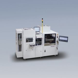
    One of the hidden champions is the wafer printing cell. A highly efficient system for processing wafers. Depending on the process stage, the wafers can be coated over a wide area or tens of thousands of bumps can be printed.

    The flexible machining cell is designed for front or back side printing (bumping or wafer backside coating) on round wafers. The system consists of two main modules, a loading unit and a printing system. The loading unit consists of three components: a magazine unloading system, a robot unit and a pre-alignment station. The magazine unloading system is equipped with two magazine positions from where the wafers are fed to the machine. The 3-axis robot unit with vacuum suction pad ensures a stress-free wafer transport. Using a flexible pick-up, different end effectors can be used even for very thin or curved wafers. After the wafer is removed from the magazine, it is repositioned in the pre-alignment station by flat or notch detection for subsequent printing. Now, the wafer is placed on dedicated elevation pins of the vacuum print nest and then lowered and fixed. The print nest is transported into the printer. Then the register marks are detected by the free-moving camera and the screen or stencil is aligned to the wafer. The printing process is then carried out. The printed wafer is now transported back into a magazine or can be removed individually with a drawer system.
    Subsequent process steps, such as heat treatment, can be integrated in or on the cell at the customer’s request.


    Mehr aus Semiconductor-packaging

    Weitere aktuelle Artikel aus der Rubrik Semiconductor-packaging.

    Alle Semiconductor-packaging-Artikel
    Nanoscribe Expands Photoresin Portfolio for Micro-Optics Fabrication via Two-Photon PolymerizationFoto: Brecht Corbeel / Unsplash
    Semiconductor-packaging

    Nanoscribe Expands Photoresin Portfolio for Micro-Optics Fabrication via Two-Photon Polymerization

    11. November 2026

    Nanoscribe has detailed its range of photoresins engineered for Two-Photon Polymerization (2PP) and Two-Photon Grayscale Lithography (2GL), targeting high-precision micro-optics manufacturing on silicon, glass, and…

    Canon Launches FPA-6400ES6a KrF Lithography System with 400 Wafers-per-Hour ThroughputFoto: Canon Europe (semicon)
    Semiconductor-packaging

    Canon Launches FPA-6400ES6a KrF Lithography System with 400 Wafers-per-Hour Throughput

    10. November 2026

    Canon has announced the FPA-6400ES6a KrF scanner for semiconductor lithography, combining a throughput of 400 wafers per hour with industry-leading overlay accuracy of 4.0 nm and the ability to handle wafer warpage of…

    Fabmatics absorbs SCI business activities under unified brandFoto: Ludovico Ceroseis / Unsplash
    Semiconductor-packaging

    Fabmatics absorbs SCI business activities under unified brand

    6. November 2026

    Fabmatics has integrated the business activities of SCI under the Fabmatics brand, consolidating the acquired expertise within its semiconductor automation portfolio.

    Entegris and Kioxia Expand Partnership on Materials Innovation for Next-Gen 3D Flash MemoryFoto: Louis Reed / Unsplash
    Semiconductor-packaging

    Entegris and Kioxia Expand Partnership on Materials Innovation for Next-Gen 3D Flash Memory

    6. November 2026

    Entegris and Kioxia are deepening their strategic partnership to co-develop materials and process technologies for future BiCS FLASH 3D NAND architectures, using AI, digital-twin modelling and experimental validation at…

    ← Zurück zu Semiconductor-packagingZur Startseite

