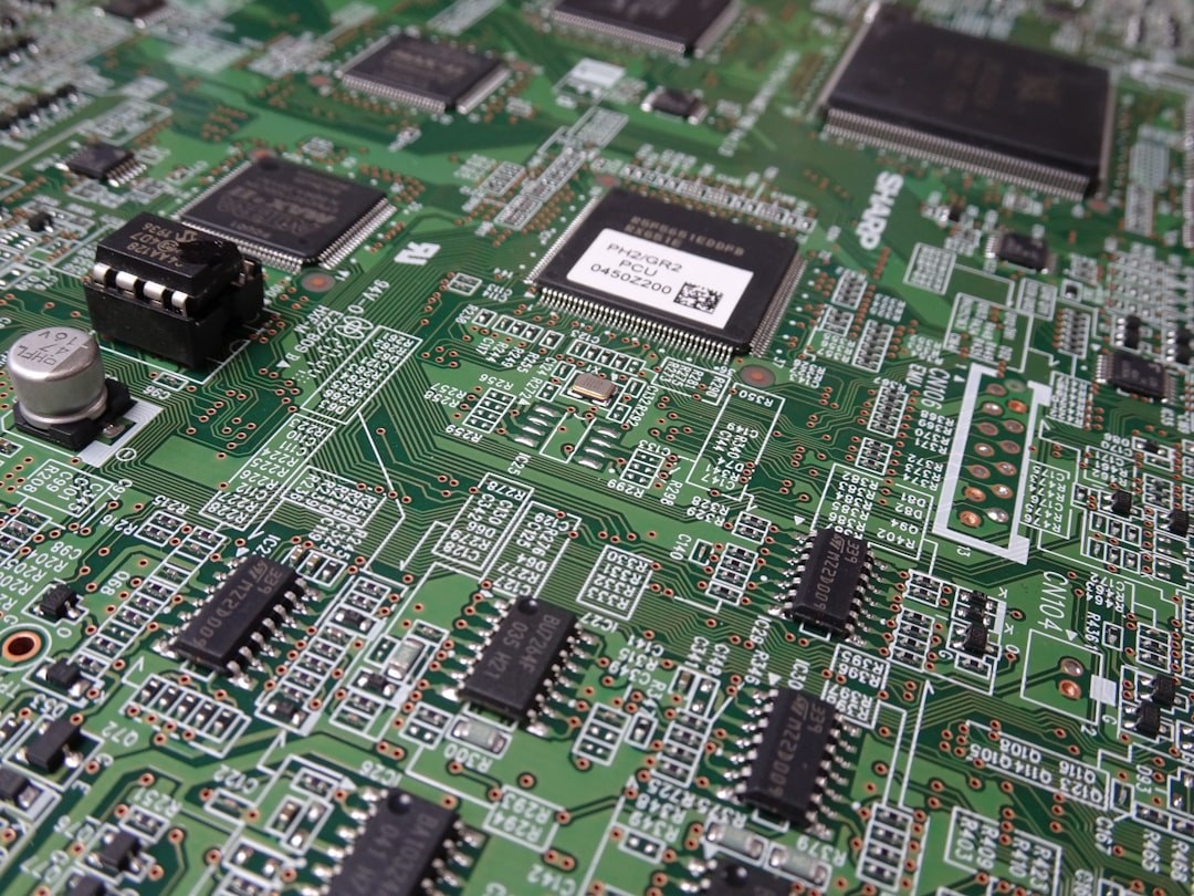
Modern printed circuit board assemblies rarely consist of surface-mount components alone. Connectors, press-fit terminals, transformers and electromechanical parts frequently require through-hole mounting, creating a soldering challenge when sensitive SMT components or heat-critical substrates occupy the same board. Wave soldering exposes the entire underside of the board to a molten solder bath, which can damage already-placed SMDs, flux residues or thermally sensitive plastics. Hand soldering, by contrast, is slow, operator-dependent and difficult to control statistically. Selective soldering was developed specifically to address this conflict, applying solder precisely where it is needed and nowhere else.
The technology has matured considerably over the past two decades and is today a standard process step in automotive electronics, industrial control, telecom infrastructure and medical device manufacturing — anywhere that through-hole components coexist with fine-pitch SMT on the same assembly. A solid grasp of the underlying principles allows process engineers to choose the right machine architecture, define appropriate process windows and avoid the most common failure modes.
Machine Architectures: Nozzle, Mini-Wave and Laser
Three principal machine concepts dominate the selective soldering market. The most widely deployed is the single-point or multi-point nozzle system, in which a small fountain nozzle — typically 4 mm to 25 mm in diameter — pumps molten solder upward through a precisely controlled orifice. The board is programmed to move over the nozzle, or the nozzle moves beneath a stationary board, dwelling at each through-hole location for a defined time. This approach offers excellent repeatability and is well suited to high-volume production of boards with a modest number of through-hole sites.
The second architecture uses a drag soldering or mini-wave concept, where a small elongated wave is dragged along a defined path, soldering entire rows of pins — connector footprints, for example — in a single pass. Throughput is higher for linear pin fields, but the process is less flexible for scattered component placements. The third and emerging architecture uses a focused laser beam to melt solder wire or a pre-deposited solder perform directly at the joint. Laser selective soldering avoids any contact with the solder bath and is particularly attractive for extremely heat-sensitive substrates or when nitrogen-free, low-oxygen soldering is impractical. Each architecture involves different thermal dynamics and demands different process qualification strategies.
Flux Application: The Foundation of Joint Quality
Regardless of machine type, fluxing is the first active process step and arguably the most critical. Selective flux systems apply flux only to the specific through-hole pads rather than coating the entire board underside as a wave fluxer would. The three common flux delivery methods are drop-jet (piezo-driven droplet dispensing), spray fluxing through a miniature nozzle, and pin-transfer systems. Drop-jet fluxing is the most precise, placing individual droplets of 20 µl to 100 µl with positional accuracy better than 0.1 mm, which is important for preventing flux contamination of adjacent SMD components or connectors with sealing requirements.
Flux selection for selective soldering follows the same IPC J-STD-004 classification framework used for other soldering processes. No-clean fluxes of the ROL0 and REL0 categories are preferred in most industrial applications because flux residues under through-hole components can be virtually impossible to clean. However, the flux must still be thermally activated and fully volatilised during the soldering dwell time; insufficient activation temperature or too short a dwell leads to dewetting, voiding and disturbed joints. Flux volume, spread factor and activator content must be validated against the actual solder temperature and dwell time used in production.
Thermal Management: Preheating and Solder Temperature
Through-hole soldering demands that sufficient heat energy reaches the barrel wall, the lead and the pad simultaneously. A cold barrel absorbs thermal energy from the solder fountain and can prevent the solder from wetting fully before it is pulled away by gravity and surface tension. Preheating the board — typically to 100 °C to 130 °C on the top side — reduces the thermal delta the solder nozzle must overcome and helps activate the flux. Bottom-side preheating is also used to reduce thermally induced bow and to stabilise the solder temperature in the nozzle pool itself.
Solder bath temperature in selective systems typically ranges from 260 °C to 290 °C for Sn-Ag-Cu lead-free alloys, slightly higher than equivalent wave soldering temperatures because the nozzle pool has a smaller thermal mass and cools more rapidly when contacting a cold board section. The dwell time — the period during which the board pad remains in contact with the solder fountain — is the primary process variable for controlling heat input. Typical dwell times range from 2 seconds to 8 seconds per joint cluster; dwell times beyond 10 seconds risk intermetallic growth, pad lifting or damage to thermoplastic connector bodies.
Common Defect Mechanisms and Their Root Causes
Bridging between adjacent pins is the most frequently reported selective soldering defect and is almost always traceable to one of three causes: excessive flux volume creating a flux bridge that carries solder across the gap; solder drip or satellite formation as the nozzle retracts; or incorrect nozzle geometry relative to pin pitch. Icicles and solder peaks result from too-rapid nozzle retraction or insufficient solder volume during the fill phase, leaving a pull-off tail that solidifies before it can drain. Non-wetting or dewetting indicates either inadequate flux activation, oxide contamination on the lead or pad, or solder temperature that is too low relative to the thermal mass of the component.
Voiding inside the barrel — detectable only by X-ray inspection — is caused by outgassing from plating residues, moisture absorbed into the PCB laminate or entrapped flux volatiles. Baking boards at 105 °C for two to four hours prior to soldering is a well-established countermeasure for moisture-related voiding. IPC-A-610 defines acceptance criteria for through-hole solder joint fill, requiring a minimum of 75 % vertical fill of the barrel for Class 2 assemblies and 100 % for Class 3, which makes process window definition particularly important for medical or aerospace applications.
Nitrogen Atmosphere and Alloy Selection
Selective soldering machines can be operated in air or under a local nitrogen shroud around the nozzle. A nitrogen blanket reduces oxidation of the solder bath surface and the nozzle tip, lowers dross formation and generally allows a wider process window with smaller flux volumes. For lead-free alloys with higher tin content — which are inherently more oxidation-prone than eutectic Sn-Pb — nitrogen becomes particularly beneficial. Oxygen levels below 500 ppm in the nozzle zone are a common industry target; some processes targeting zero-flux or minimal-flux applications require levels below 100 ppm.
Alloy choice affects joint reliability as well as process parameters. SAC305 (Sn-3.0Ag-0.5Cu) remains the dominant lead-free alloy in selective soldering, but low-silver alloys such as SAC0307 and bismuth-containing alloys are gaining ground where cost, thermal fatigue resistance or low-temperature processing are priorities. Bismuth-containing solders require careful management because even trace amounts of lead contamination — from leaded component finishes mixing with bismuth alloy — can form a low-melting ternary eutectic at 96 °C, which is a known reliability risk in field-temperature-cycling environments.
Process Qualification, Control and Outlook
Establishing a robust selective soldering process begins with a design-for-manufacturability review: component placement clearances to SMDs, pad annular ring dimensions, board thickness and copper barrel plating thickness all influence the achievable process window. IPC-7711/7721 and IPC-A-610 provide the reference framework for joint acceptance, while IPC-7530 addresses guidelines for thermal profiling of soldering processes. Statistical process control of key parameters — nozzle temperature, flux deposit volume, preheat temperature and dwell time — combined with automated optical inspection of the soldered joints, provides the closed-loop feedback necessary for Cpk values that satisfy automotive IATF 16949 or medical ISO 13485 quality management requirements.
Looking ahead, the integration of selective soldering machines into MES-driven smart production lines is increasing the demand for inline traceability: each joint cluster can be linked to measured process data, enabling full genealogy from board serial number to soldering parameters. Vision-based joint inspection directly at the nozzle, real-time flux deposit verification and AI-assisted defect classification are progressively moving selective soldering from a manually tuned process toward a fully data-driven one — a shift that is likely to define best practice in through-hole soldering for the coming generation of high-reliability electronics.