
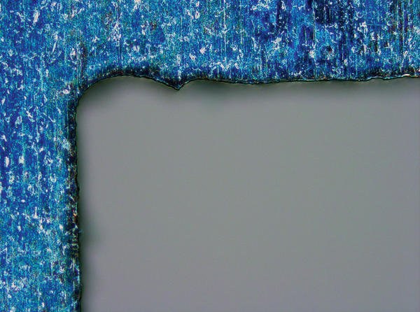
The advancing miniaturization of components requires increasingly accurately positioned and defined solder paste and adhesive deposits, and the surfaces of the materials used affect the printing results significantly. Improvements are being made in all phases of stencil production: in the data processing phase, the stencil production phase and the stencils surface design. In the data processing phase, openings are reduced, rounded and split, and special shapes are used to prevent tombstones or solder beads. The subsequent stencil production involves a lot more than just “cutting holes”. Instead, air conditioned production environments are just as indispensable today as is the reduction of cutting speeds, particularly in fine pitch applications. Optimum parameters in stencil production form the basis for stable and reproducible manufacturing processes at the customer. The stencil printing process is predominantly defined by four interfaces some of which can be directly affected and logically combined during stencil production: stencil top, squeegee surface, aperture wall and stencil bottom. Each interface must perform specific tasks:
Depending on the condition of the stencil top and the squeegee speed, the printing medium is placed into a rolling movement of varying intensity. This rolling movement enables the printing medium to squeeze through the aperture almost vertically and leads to the temporary reduction of its viscosity that enables it to completely fill even small apertures.
If the printing medium is unable to find sufficient support on the stencil surface, for example because of excessive squeegee speed or insufficient surface roughness, it doesn’t roll and the apertures are not completely filled. That’s why the stencil surface must be designed to provide optimum support for the printing medium so that it can be efficiently “rolled” by the squeegee.
As the squeegee pushes the printing medium across the stencil, the squeegee’s angle generates back pressure in the medium. The squeegee’s surface counteracts the rolling movement, but generates the medium’s back pressure based on the squeegee’s speed, angle and roughness. The squeegee’s angle has the greatest impact on the back pressure.
It is nevertheless important to strike a good balance between the medium’s friction and slip at the squeegee’s surface. This can be accomplished with grinding or polishing as well as with certain surface coatings. The medium’s flow behavior determines the right surface selection.
The aperture wall defines the deposit volume and is the critical factor for a stencils release behavior. Even if the aperture was completely filled during the printing process, an imbalanced ratio of wall surface and area (area ratio) can cause some of the paste to remain in the opening. When printing adhesives, this may sometimes be desirable, but when printing solder paste it creates problems. The minimum area ratio that ensures the complete release of the solder paste from the aperture is around > 0.66. This value requires, however, that the aperture walls are smooth and enable perfect release behavior. The roughness of the aperture wall is determined predominantly by the stencils manufacturing method. Because of their manufacturing process, laser cut stencils have a certain basic roughness that is created during the cutting process. Depending on the choice of cutting parameters, the roughness of the aperture walls can vary considerably. If applied correctly, subsequent surface treatment methods can further reduce the aperture walls roughness and improve the stencils release characteristics. Examples of such processes include electropolishing or the application of an additional non stick coating. You must make sure, however, that all components can be placed correctly with the resulting increase in paste volume.
Stepped stencils provide an additional component related adjustment of the stencil thickness. With stepped stencils you can optimize the area ratio and apply the correct paste volume for each component. When using a stepped stencil, the distance should not be less than 36 times the step height from the step’s edge for small apertures (see IPC-7525A). Depending on the squeegee used and the component mix, this value may vary.
Together with the substrate surface, the stencil bottom seals the aperture and prevents the printing medium from creeping underneath the stencil. The stencil bottom should be as smooth as possible so that full contact can be made with the pad. Polishing provides the best results. One desirable side effect is the condition of the stencil bottom also determines the cleaning effort for the stencil in the printer. Polished surfaces reduce the time spent for this procedure considerably. Nonstick coatings may also be used, because they prevent the flux from creeping to the bottom of the stencil.
The stencils surface treatment has a major impact on the printing characteristics. Intelligently combining these factors produces better printing behavior and optimizes the process conditions in electronics production. On the other hand, making the wrong choice for only one of the four interfaces can ruin an otherwise excellent stencil and be the cause of quality problems in the overall process.
EPP Europe 441
Die Miniaturisierung der Bauelemente erfordert immer exakter positionierte und definierte Lot- und Kleberdepots. Die Auswahl der Oberflächenbehandlungen an der Schablone hat einen wesentlichen Einfluss auf ihr Druckverhalten. Eine geschickte Kombination bewirkt ein stabileres Druckverhalten und optimale Prozessbedingungen für die Elektronikfertigung. Mit präzisen Stufenschablonen lässt sich die Schablonendicke Bauteil bezogen optimieren.
La miniaturisation des composants exige une définition et un positionnement toujours précis des dépôts de brasure et de colle. Le choix des traitements de surface des pochoirs influence considérablement leur comportement à l’impression. Une combinaison appropriée entraîne un comportement à l’impression plus stable et des conditions de process optimales pour la fabrication de composants électroniques. L’utilisation de pochoirs étagés précis permet d’optimiser l’épaisseur du pochoir par rapport au composant.
La miniaturizzazione dei componenti esige depositi di saldatura e di collante posizionati e definiti con una precisione sempre maggiore. La scelta dei trattamenti superficiali sullo stencil influisce sensibilmente sul suo comportamento alla pressione. Un’abile combinazione produce un comportamento più stabile alla pressione e condizioni di processo ottimali per la produzione del componente elettronico. Con precise sagome a gradini è possibile ottimizzare lo spessore dello stencil in riferimento al componente.



