
Zum Inhalt springen
EPP Europe
  • News
  • Products
  • Applications
  • Technology
  • Semiconductor
  • Inspection
  • Company News
  • Events
EPP Europe
  • Technology
  • Inspection (AOI/AXI)
  • Semiconductor Packaging
  • Company News
  • Products
  • Trade Shows & Events
    EPP Europe Newsletter
    The most important electronics-manufacturing news delivered to your inbox.

    Info

    • Impressum
    • Datenschutz
    • Barrierefreiheit
    • Datenschutzeinstellungen

    Kontakt zur Redaktion

    EPP EuropeKonradin Mediengruppe
    Ernst-Mey-Str. 8, 70771 Leinfelden-Echterdingen

    E-Mail: redaktion@konradin.de
    Folgen Sie uns
    EPP Europe
    © 2026 EPP Europe
    Startseite/Semiconductor-packaging/Artikel
    Printing Requirements for Semiconductor Packaging
    Bildquelle nicht angegeben
    Semiconductor-packaging

    Printing Requirements for Semiconductor Packaging

    It is well known that modern paste printing systems are characterised by their high flexibility: The printing systems adapt dynamically to changing
    Veröffentlicht
    08. September 2022
    Lesezeit
    2 Minuten
    Rubrik
    Semiconductor-packaging

    Key factors that determine successful paste transfer are the flatness of the substrate and its coplanarity to the stencil. Coplanarity directly influences the release behaviour during the separation process. Usually, substrates are a few tenths of a millimetre thin and usually not 100% flat. Special transport and holding systems are used for such cases.

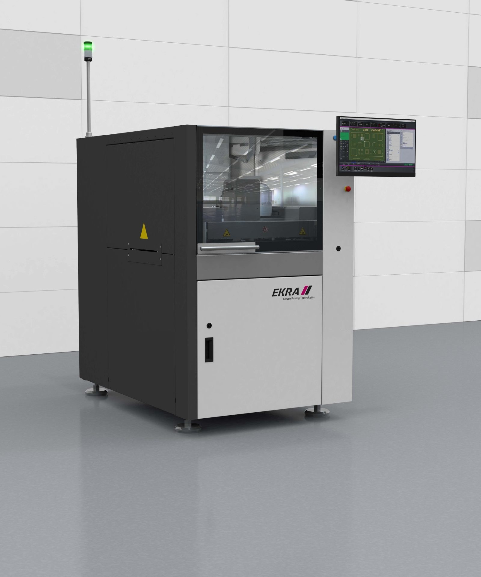
    XH2 Printing System
    XH2 Printing System
    Multiclamp 3in1 transport system
    Multiclamp 3in1 transport system

    On the one hand, the substrate must be transported securely, on the other hand, it must be fixed flat, snap-off-free and coplanar for printing. It is important that the substrate is fully supported. The result is a completely flat surface for print application.
    It goes without saying that reproducible high quality also requires reliably reproducible conditions. This depends on the design of the printing table and the camera system of the printing system.

    The camera must be able to reliably detect the smallest fiducials on varying substrate materials such as lead frames, wafers and ceramics (to name but a few). However, the system must also be able to work with synthetic fiducials and edge alignment as well. Integrated measuring systems with feedback into the positioning control loop enable micrometre-precise lateral alignment of the substrate against the stencil. This ensures optimum sealing for each individual printing process.

    But the vertical lift must also work with high precision. With stencil thicknesses in the less than 2-digit micrometre range, any overstretching can lead to stretch or destruction of the stencil. On the other hand, the printing process with solder paste type 7 or 8 requires a perfect seal. Otherwise, the solder paste, which has a grain size of less than 10µm, can escape at the unsealed areas and form bridges. Since the separation of the substrate from the stencil also has an influence on the print result, high-resolution servo motor drives must be used here as well. In this way, the release behaviour of the paste can be optimised as well.

    To be able to print ultra-fine-pitch applications perfectly, the printing unit, the print head, must be designed for this. Sufficient printing force, continuously controlled, must be available to ensure ideal filling behaviour. Printing force and speed must be reproducible, as this has a direct influence on the filling level and print volume. The EKRA Autohead, combines motor-driven stroke & pneumatic controlled squeegee pressure. In addition, the stencil must be force-relieved before the separation process in order not to negatively influence the coplanarity during the separation process.


    Mehr aus Semiconductor-packaging

    Weitere aktuelle Artikel aus der Rubrik Semiconductor-packaging.

    Alle Semiconductor-packaging-Artikel
    Nanoscribe Expands Photoresin Portfolio for Micro-Optics Fabrication via Two-Photon PolymerizationFoto: Brecht Corbeel / Unsplash
    Semiconductor-packaging

    Nanoscribe Expands Photoresin Portfolio for Micro-Optics Fabrication via Two-Photon Polymerization

    11. November 2026

    Nanoscribe has detailed its range of photoresins engineered for Two-Photon Polymerization (2PP) and Two-Photon Grayscale Lithography (2GL), targeting high-precision micro-optics manufacturing on silicon, glass, and…

    Canon Launches FPA-6400ES6a KrF Lithography System with 400 Wafers-per-Hour ThroughputFoto: Canon Europe (semicon)
    ← Zurück zu Semiconductor-packagingZur Startseite
    Autohead
    Autohead

    All relevant print parameters can be transferred to the downstream SPI via an interface. This allows complex control loops to be set up for process optimisation, which automatically optimise the printing or separating behaviour in a targeted manner, without any intervention by the operating personnel.

    ASYS Group

    Semiconductor-packaging

    Canon Launches FPA-6400ES6a KrF Lithography System with 400 Wafers-per-Hour Throughput

    10. November 2026

    Canon has announced the FPA-6400ES6a KrF scanner for semiconductor lithography, combining a throughput of 400 wafers per hour with industry-leading overlay accuracy of 4.0 nm and the ability to handle wafer warpage of…

    Fabmatics absorbs SCI business activities under unified brandFoto: Ludovico Ceroseis / Unsplash
    Semiconductor-packaging

    Fabmatics absorbs SCI business activities under unified brand

    6. November 2026

    Fabmatics has integrated the business activities of SCI under the Fabmatics brand, consolidating the acquired expertise within its semiconductor automation portfolio.

    Entegris and Kioxia Expand Partnership on Materials Innovation for Next-Gen 3D Flash MemoryFoto: Louis Reed / Unsplash
    Semiconductor-packaging

    Entegris and Kioxia Expand Partnership on Materials Innovation for Next-Gen 3D Flash Memory

    6. November 2026

    Entegris and Kioxia are deepening their strategic partnership to co-develop materials and process technologies for future BiCS FLASH 3D NAND architectures, using AI, digital-twin modelling and experimental validation at…

