
Zum Inhalt springen
EPP Europe
  • News
  • Products
  • Applications
  • Technology
  • Semiconductor
  • Inspection
  • Company News
  • Events
EPP Europe
  • Technology
  • Inspection (AOI/AXI)
  • Semiconductor Packaging
  • Company News
  • Products
  • Trade Shows & Events
    EPP Europe Newsletter
    The most important electronics-manufacturing news delivered to your inbox.

    Info

    • Impressum
    • Datenschutz
    • Barrierefreiheit
    • Datenschutzeinstellungen

    Kontakt zur Redaktion

    EPP EuropeKonradin Mediengruppe
    Ernst-Mey-Str. 8, 70771 Leinfelden-Echterdingen

    E-Mail: redaktion@konradin.de
    Folgen Sie uns
    EPP Europe
    © 2026 EPP Europe
    Startseite/News/Artikel
    Photonics specialist expands in Jena
    Bildquelle nicht angegeben
    News

    Photonics specialist expands in Jena

    A high-end manufacturing facility for semiconductor optics will be expanded at Jenoptik’s production campus in Jena. The photonics group will invest an
    Veröffentlicht
    10. September 2025
    Lesezeit
    2 Minuten
    Rubrik
    News

    The expanded production areas will be used by the company to manufacture sophisticated, high-quality optical components that are mainly used in the semiconductor equipment industry. Once preliminary planning is completed by the end of 2025 and the subsequent approvals and contracts are granted, the renovation of the currently vacant hall is scheduled to begin in summer 2026. Production in the new manufacturing environment is scheduled to start in the second half of 2027.

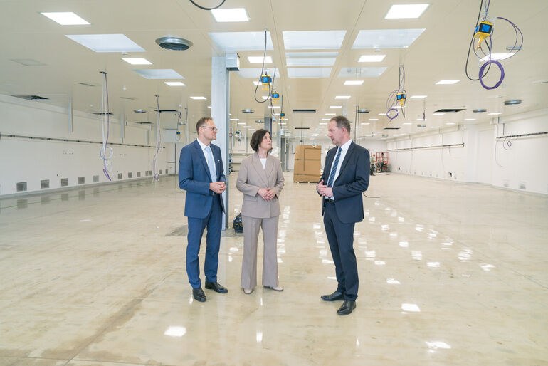
    The company’s President and CEO, Dr Stefan Traeger, and Colette Boos-John, Thuringia’s Minister for Economic Affairs, Agriculture and Rural Areas, announced the planned investment on September 9.

    The comprehensive renovation is planned in two stages. First, an area of around 2,000 sqm will be modularly expanded and modernized, also with regard to energy efficiency, to accommodate the additional production capacity. An additional expansion in line with demand is possible depending on medium-term growth, particularly with customers in the semiconductor equipment industry, and taking into account the requirements for the global alignment of manufacturing capacities. Investments in state-of-the-art machinery and infrastructure are planned.

    The refurbished hall will ultimately offer state-of-the-art space for the production of high-end optics, an essential component of high-performance photonic modules and systems. In addition to growth, the investment will also enable an even stronger focus on modern value stream concepts. This will optimize material flows in optics component manufacturing, make processes more efficient and transparent—while maintaining the highest quality standards.

    Dr Traeger commented: “With this investment in one of our core businesses, we are responding to the increasing demands of our customers in the growth area of semiconductor technology. Furthermore, the investment is a commitment to our main location in Jena, where we are part of a unique ecosystem in the photonics industry in which business, research institutes, and universities collaborate and important structures for suppliers, training, and qualified specialists are available.”

    Earlier this year, Jenoptik opened a new high-tech factory in Dresden, Germany, in an area known as “Silicon Saxony”. At the site, micro-optics and sensors for the semiconductor equipment industry are being produced.

    “The optics industry remains a growth sector for Thuringia,” commented Boos-John. “In view of the current economic sideways movement in Germany, it is a strong signal that Jenoptik is now also investing at its Thuringian headquarters. This demonstrates fundamental confidence in the location, which we must justify at the federal and state level by further improving the economic framework conditions.” The minister added that the state of Thuringia will continue to monitor and support the development of Jenoptik, one of its flagship companies.


    www.jenoptik.com

    Mehr aus News

    Weitere aktuelle Artikel aus der Rubrik News.

    Alle News-Artikel
    Microtronic Takes on Distribution of iRaptor EYE Thermal Profiler in GermanyFoto: Laurens van der Drift / Unsplash
    News

    Microtronic Takes on Distribution of iRaptor EYE Thermal Profiler in Germany

    9. November 2026

    German distributor Microtronic has announced it will represent iRaptor LDA and its EYE thermal profiler in Germany. The Portuguese developer's system extends beyond conventional 2D time-temperature profiling by…

    Indium Corporation Presents Solder Materials Research at SMTAI 2026Foto: Indium Corporation
    News

    Indium Corporation Presents Solder Materials Research at SMTAI 2026

    29. Oktober 2026

    Indium Corporation is fielding five specialists at SMTA International 2026 to present new findings on solder paste rheology, BGA ball alloy selection for lower-temperature reflow, and the effect of print gap on paste…

    KYZEN to Present AQUANOX Aqueous Cleaning Chemistries at SMTA International 2026Foto: Vishnu Mohanan / Unsplash
    News

    KYZEN to Present AQUANOX Aqueous Cleaning Chemistries at SMTA International 2026

    16. Oktober 2026

    KYZEN will exhibit its AQUANOX line of aqueous electronics cleaning chemistries at SMTA International, October 27–29, 2026, highlighting prolonged bath life as a process efficiency and cost-reduction lever for…

    Fuji America and Cybord Partner to Integrate Visual AI Component Inspection into SMT LinesFoto: Cybord
    News

    Fuji America and Cybord Partner to Integrate Visual AI Component Inspection into SMT Lines

    29. August 2026

    Fuji America Corporation and Cybord have announced a strategic partnership to embed AI-powered component analytics directly into SMT production lines, enabling 100% real-time inspection of electronic components during…

    ← Zurück zu NewsZur Startseite

