
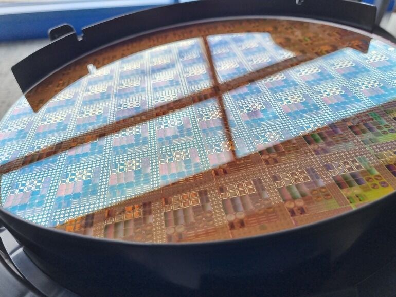
The agreement, signed between STMicroelectronics and Metalenz, broadens the former’s capability to use Metalenz’s intellectual property to produce advanced metasurface optics while leveraging its own unique technology and manufacturing platform combining 300 mm semiconductor and optics production, test and qualification.
“Since 2022, we have shipped well over 140 million metasurface optics and FlightSense modules using Metalenz IP. The new license agreement bolsters our technology leadership in consumer, industrial and automotive segments, and will enable new opportunities,” commented Alexandre Balmefrezol, Executive Vice President and General Manager of STMicroelectronics’s Imaging Sub-Group. He added: “Our unique model, processing optical technology in our 300 mm semiconductor fab, ensures high precision, cost-effectiveness, and scalability to meet the requests of our customers for high-volume, complex applications.”
Rob Devlin, co-founder and CEO of Metalenz, commented: “Our agreement has the potential to further fast-track the adoption of metasurfaces from their origins at Harvard to adoption by market leading consumer electronics companies.” He added: “By enabling the shift of optics production into semiconductor manufacturing, this agreement has the possibility to further redefine the sensing ecosystem.”
The new license agreement aims to address the growing market opportunity for metasurface optics, which is projected to experience significant growth to reach $2B by 2029; largely driven by the industry’s role in emerging display and imaging applications.
In 2022, metasurface technology from Metalenz, which spun out of Harvard and holds the exclusive license rights to the foundational Harvard metasurface patent portfolio, debuted with ST’s market leading direct Time-of-Flight (dToF) FlightSense modules.
Replacing the traditional lens stacks and shifting to metasurface optics instead has improved the optical performance and temperature stability of the FlightSense modules while reducing their size and complexity.
The use of 300 mm wafers ensures high precision and performance in optical applications, as well as the inherent scalability and robustness advantage of semiconductor manufacturing process.



