
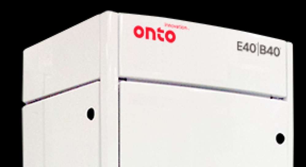
New EB40 tool expands the Company’s process control market for advanced logic and memory wafers.
Onto Innovation Inc. (NYSE: ONTO) (“Onto Innovation,” “Onto,” or the “Company”) today announced its rst shipment of the Company’s Dragony G3 system with the new EB40 module to a top three semiconductor manufacturer. Together, the system and module oer all-surface wafer inspection to address the yield loss caused by defects on the wafer edge and backside across front-end and backend processes.
All-surface inspection is becoming critical for quality assurance at foundries and IDMs producing advanced packages. The prevalence of edge-handling equipment needed to accommodate thinner wafers can produce chips and cracks that potentially propagate into the die near the wafer’s edge, which becomes a costly loss on a nished wafer. That’s where the 30% greater sensitivity and twice the throughput of the integrated Dragony G3 system and EB40 module come in.
Onto Innovation’s new EB40 solution provides not only the required sensitivity to identify these defects at high speed but also oers the analytics software, such as Onto’s ADC (automatic defect classication), to determine the defect type, impact and, in some cases, origin. Yole Group estimates AI and HPC architectures will grow by greater than 30% over the next three years. Based on these estimates and the strong positive customer reception we have seen in the initial release of the Dragony G3 system with the EB40 module, we expect this new capability to result in a process control SAM expansion for advanced logic and memory.
Wafer fab in-line process control requirements and BEOL nal outgoing quality inspection are needed for the development of advanced node architectures in logic as well as emerging memory segments. This new market opportunity is in addition to the advanced packaging market where the combination of the Dragony G3 system and EB40 module is adding all-surface inspection to the Dragony G3 system’s tool-of-record status at the top
manufacturers.
“A top-tier memory customer commented that front-end wafer processing cycle times are extending to several months, and they are trying to ensure that yield issues are not going undetected at their fabs. As a result, a lot of focus is now being placed on early detection of potential yield issues and inspection, including edge and backside,” commented Damon Tsai, director of product management within Onto Innovation’s inspection business.
He continued, “Early inspection of the wafer edge is especially critical since small edge cracks can potentially propagate into the die near the wafer perimeter. This is particularly important since the large size of these new devices means there are fewer chips per wafer, so any yield loss resulting from rejected die can be signicant. Of course, the Dragony G3 system is also ideal for nal outgoing quality assurance since the tool oers the final product inspection point for wafers moving to the packaging facility.”
The integration of the Dragony G3 system with the EB40 module not only introduces backside edge bead-removal metrology, but also oers a signicant shift in sensitivity enabled by a new algorithm for defect detection, allowing this powerful duo of tools to exceed on-wafer needs and nd backside scratches, color variations and large particles that can cause advanced packaging defects. The Dragony G3 system with the EB40 module is capable of
doubling the number of wafers per hour oered by previous tools, while allowing manufacturers to detect residue and particles on the wafer surface with superior precision.
Volume purchase agreements and orders for the Dragony G3 system and EB40 module are part of the Company’s previously stated outlook for 2022.



