
Zum Inhalt springen
EPP Europe
  • News
  • Products
  • Applications
  • Technology
  • Semiconductor
  • Inspection
  • Company News
  • Events
EPP Europe
  • Technology
  • Inspection (AOI/AXI)
  • Semiconductor Packaging
  • Company News
  • Products
  • Trade Shows & Events
    EPP Europe Newsletter
    The most important electronics-manufacturing news delivered to your inbox.

    Info

    • Impressum
    • Datenschutz
    • Barrierefreiheit
    • Datenschutzeinstellungen

    Kontakt zur Redaktion

    EPP EuropeKonradin Mediengruppe
    Ernst-Mey-Str. 8, 70771 Leinfelden-Echterdingen

    E-Mail: redaktion@konradin.de
    Folgen Sie uns
    EPP Europe
    © 2026 EPP Europe
    Startseite/News/Artikel
    Ongoing expansion/miniaturization
    Bildquelle nicht angegeben
    News

    Ongoing expansion/miniaturization

    Good to know that there still is consensus in the world – in the world of semiconductor devices and manufacturing, that is. Take a look at the
    Veröffentlicht
    02. November 2004
    Lesezeit
    2 Minuten
    Rubrik
    News

    This year, in the two-year chip innovation cycle, the ITRS is only an update of last year’s edition, to be edited and co-developed by about 1000 industry volunteers and to be finished soon now, before it becomes the global planning tool for the high-tech industry. Yet, in the regular flow of things, the 2004 ITRS update has created an unusual ruckus. Why? It spells out, in the words of its chairman Paolo Gargini (also director of technology strategy at Intel), a path to and the timetable for nanotechnology in chip manufacturing. And, even more disturbing to equipment makers, it initiates the migration to a wafer diameter of 450mm, to be production-ready in 2012.

    In other words: the headache of migrating to 300mm will return, but much bigger. In the “proposed 450mm-wafer transition timeline” (Gargini in his keynote speech at Semicon West 2004), next year will see the first wafer standards evolving as well as the determination of carrier and lot-sizes. In 2006, just when the next chip recession is probably going to roll around, the industry will have to deal with new and more expensive factory control systems, transport and equipment standards – all to continue through 2010. Then it’ll time for the first 450mm alpha tools to arrive and begin a three-year cycle of interoperability testing and reliability verification. It took seven years of definitions and pilot production for 300mm to almost arrive in mainstream semiconductor production, Gargini says. “For a 2012 intercept that means that the analysis should begin in 2005”. And that’s not all of it, folks. As one of Gargini’s statements revealed, the next monster wafer size – only a joke? – is waiting around the corner: 675mm-diameter wafers are supposed to arrive in 2019.

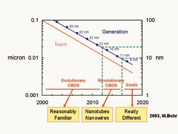
    The other key element of the update is the timeline to nano devices, tools and materials. Until 2010, Gargini contends, “evolutionary CMOS” will continue: with downscaling as usual, but with new ingredients such as strained Si, high-k gate dielectrics, metal-gate electrodes, advanced MOSFETs (FDSOI) and enhanced v-sat devices with quasi-ballistic charge transport mechanisms. Then, around 2012, “revolutionary” CMOS will step up on the stage: with nanotubes and nanowires, optical interconnect and molecular self-assembly replacing mechanical pick-and-place. To be followed by “exotic” devices. Which, that much is known today, will be “really different.” Stay tuned for single-transistor switches and spintronics. Just what kind of exotic, really different manufacturing tools will all this require? In time, we will know a bit more on this predicted technology future.

    Werner Schulz

    EPP EUROPE 404

    www.public.itrs.net

    Mehr aus News

    Weitere aktuelle Artikel aus der Rubrik News.

    Alle News-Artikel
    Microtronic Takes on Distribution of iRaptor EYE Thermal Profiler in GermanyFoto: Laurens van der Drift / Unsplash
    News

    Microtronic Takes on Distribution of iRaptor EYE Thermal Profiler in Germany

    9. November 2026

    German distributor Microtronic has announced it will represent iRaptor LDA and its EYE thermal profiler in Germany. The Portuguese developer's system extends beyond conventional 2D time-temperature profiling by…

    Indium Corporation Presents Solder Materials Research at SMTAI 2026Foto: Indium Corporation
    News

    Indium Corporation Presents Solder Materials Research at SMTAI 2026

    29. Oktober 2026

    Indium Corporation is fielding five specialists at SMTA International 2026 to present new findings on solder paste rheology, BGA ball alloy selection for lower-temperature reflow, and the effect of print gap on paste…

    KYZEN to Present AQUANOX Aqueous Cleaning Chemistries at SMTA International 2026Foto: Vishnu Mohanan / Unsplash
    News

    KYZEN to Present AQUANOX Aqueous Cleaning Chemistries at SMTA International 2026

    16. Oktober 2026

    KYZEN will exhibit its AQUANOX line of aqueous electronics cleaning chemistries at SMTA International, October 27–29, 2026, highlighting prolonged bath life as a process efficiency and cost-reduction lever for…

    Fuji America and Cybord Partner to Integrate Visual AI Component Inspection into SMT LinesFoto: Cybord
    News

    Fuji America and Cybord Partner to Integrate Visual AI Component Inspection into SMT Lines

    29. August 2026

    Fuji America Corporation and Cybord have announced a strategic partnership to embed AI-powered component analytics directly into SMT production lines, enabling 100% real-time inspection of electronic components during…

    ← Zurück zu NewsZur Startseite


