
Zum Inhalt springen
EPP Europe
  • News
  • Products
  • Applications
  • Technology
  • Semiconductor
  • Inspection
  • Company News
  • Events
EPP Europe
  • Technology
  • Inspection (AOI/AXI)
  • Semiconductor Packaging
  • Company News
  • Products
  • Trade Shows & Events
    EPP Europe Newsletter
    The most important electronics-manufacturing news delivered to your inbox.

    Info

    • Impressum
    • Datenschutz
    • Barrierefreiheit
    • Datenschutzeinstellungen

    Kontakt zur Redaktion

    EPP EuropeKonradin Mediengruppe
    Ernst-Mey-Str. 8, 70771 Leinfelden-Echterdingen

    E-Mail: redaktion@konradin.de
    Folgen Sie uns
    EPP Europe
    © 2026 EPP Europe
    Startseite/Semiconductor-packaging/Artikel
    Next-Generation WaferSense & ReticleSense Auto Teaching Systems
    Bildquelle nicht angegeben
    Semiconductor-packaging

    Next-Generation WaferSense & ReticleSense Auto Teaching Systems

    CyberOptics will launch its next-generation WaferSense Auto Teaching System (ATS2) and new ReticleSense Auto Teaching System (ATSR). ATS2 and ATSR are
    Veröffentlicht
    25. Juni 2022
    Lesezeit
    1 Minute
    Rubrik
    Semiconductor-packaging

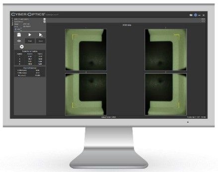
    ATS2 and ATSR are multi camera sensors used with CyberSpectrum software to teach accurate wafer and reticle hand-off calibration for proper alignment and set-up of semiconductor tools. The sensors “see” inside to capture three dimensional off-set data (x, y and z) in real-time to
    quickly teach wafer and reticle transfer positions – all without opening the tools. Process and equipment engineers can conduct repeatable and reproducible setups and maintenance checks, speed trouble-shooting and eliminate technician-totechnician variation.

    CyberSpectrum Software
    CyberSpectrum software illustrating the teach application with ATSR.

    “Semiconductor fabs worldwide are using our teaching sensors that are recognized as the most efficient and effective wireless devices for wafer hand-off teaching,” said Dr. Subodh Kulkarni, President and CEO, CyberOptics. “We have advanced the technology to enable even better performance, with the combination of accuracy, precision and versatility that fabs rely on to significantly improve their yields and tool uptime.”

    CyberOptics also will demonstrate WaferSense sensors for leveling, vibration, gapping, relative humidity, resistance and airborne particles.


    Mehr aus Semiconductor-packaging

    Weitere aktuelle Artikel aus der Rubrik Semiconductor-packaging.

    Alle Semiconductor-packaging-Artikel
    Nanoscribe Expands Photoresin Portfolio for Micro-Optics Fabrication via Two-Photon PolymerizationFoto: Brecht Corbeel / Unsplash
    Semiconductor-packaging

    Nanoscribe Expands Photoresin Portfolio for Micro-Optics Fabrication via Two-Photon Polymerization

    11. November 2026

    Nanoscribe has detailed its range of photoresins engineered for Two-Photon Polymerization (2PP) and Two-Photon Grayscale Lithography (2GL), targeting high-precision micro-optics manufacturing on silicon, glass, and…

    Canon Launches FPA-6400ES6a KrF Lithography System with 400 Wafers-per-Hour ThroughputFoto: Canon Europe (semicon)
    Semiconductor-packaging

    Canon Launches FPA-6400ES6a KrF Lithography System with 400 Wafers-per-Hour Throughput

    10. November 2026

    Canon has announced the FPA-6400ES6a KrF scanner for semiconductor lithography, combining a throughput of 400 wafers per hour with industry-leading overlay accuracy of 4.0 nm and the ability to handle wafer warpage of…

    Fabmatics absorbs SCI business activities under unified brandFoto: Ludovico Ceroseis / Unsplash
    Semiconductor-packaging

    Fabmatics absorbs SCI business activities under unified brand

    6. November 2026

    Fabmatics has integrated the business activities of SCI under the Fabmatics brand, consolidating the acquired expertise within its semiconductor automation portfolio.

    Entegris and Kioxia Expand Partnership on Materials Innovation for Next-Gen 3D Flash MemoryFoto: Louis Reed / Unsplash
    Semiconductor-packaging

    Entegris and Kioxia Expand Partnership on Materials Innovation for Next-Gen 3D Flash Memory

    6. November 2026

    Entegris and Kioxia are deepening their strategic partnership to co-develop materials and process technologies for future BiCS FLASH 3D NAND architectures, using AI, digital-twin modelling and experimental validation at…

    ← Zurück zu Semiconductor-packagingZur Startseite

