
» Jeannine Memminger-Adamski, and Kristof Hormann, Comet Yxlon
To stay ahead, manufacturers must implement comprehensive inspection strategies that enhance yield, reduce costly defects and expedite time-to-market. A crucial element of these strategies is the early detection of defects throughout critical production phases, such as wafer processing or chip level packaging. Swift identification and resolution of issues enable manufacturers to ramp up production, and advanced inspection technologies, notably 3D and 2.5D X-ray inspection, play a vital role in achieving these objectives.
3D X-ray, from lab to fab
The introduction of the CA20 by Comet in 2023 marked a significant leap forward in demonstrating the viability of 3D X-ray technology for semiconductor inspection. Bridging the gap between the speed of optical inspection and the detailed analysis provided by traditional FIB SEM, high-resolution 3D volumes can be captured in minutes, enabling manufacturers to measure and view bumps from all angles and identify critical defects such as voids, non-wet, head-in-pillow, or bump shift, and determining stand-off height to monitor die tilt or warping. In 2024, the launch of the next-generation CA20 brought this progressive technology to the production line. Featuring an EFEM loader and Automatic Defect Recognition (ADR) software powered by Dragonfly, the next-generation CA20 offers seamless integration (complaint to SECS/GEM standards) and insights that can be fed directly back into the production process.
This year, the CA20 has been further enhanced to cater to wafer inspection applications, featuring crucial design adaptations to ensure the system can safely handle delicate wafers and comply with strict cleanroom standards of up to ISO Class 1 (within the interior cabinet). With this latest release, the company has expanded its inspection portfolio to cover the entire manufacturing chain, from wafer processing to packaged chips.
3D to 2.5D –TSV inspection
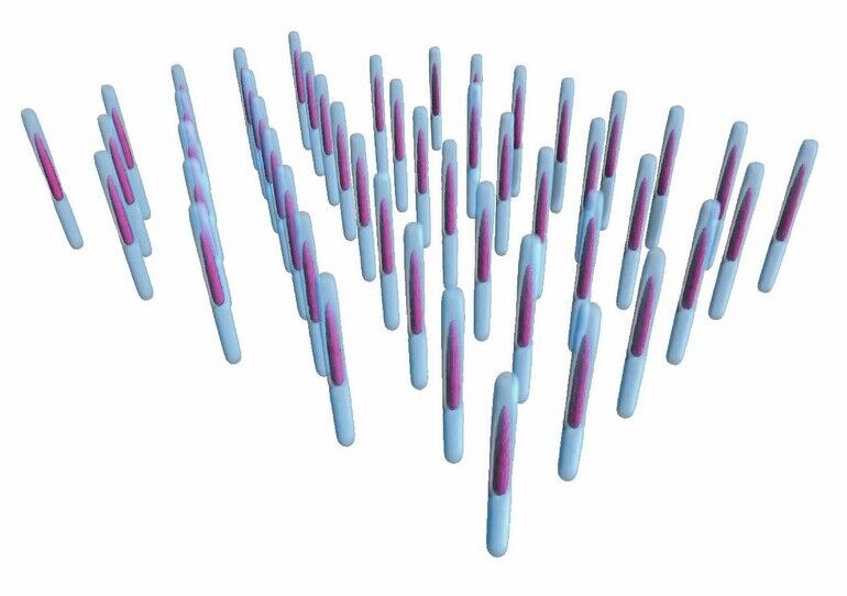
As packaging design moves into a three-dimensional space, the silicon interposer serves as an important pathway connecting functional layers. Through-Silicon Vias (TSVs) are tiny channels drilled in the interposer and typically filled with copper to establish electrical connections between bump layers. They can develop voids during the filling process, reducing electrical and thermal efficiency and potentially leading to defective connections. A single wafer can contain thousands or even millions of TSVs, tightly packed together and nearly identical in size and shape. Segmenting the individual elements and determining their position on the wafer in a consistent, reliable and efficient manner presents a significant challenge. While 3D X-ray inspection offers a full 360 ° view, perfect for the inspection of overlapping structures, for simpler TSV structures a 2.5D method can be beneficial. In this method, a 2D image is captured in several positions at a specific angle that retains sufficient depth information. This helps to determine positioning, requires less contrast to visualize any voids, and significantly reduces scan time while still presenting a statistically relevant picture of the entire wafer.
Example workflow: TSV Insights X 2.5D
This breakthrough in wafer inspection was driven by developments in the company’s AI-powered software, DirectInspect, and TSV Insights X 2.5D. This software package automatically segments the individual TSVs within the acquired X-ray images, captures critical metrological data, identifies voids and provides a classification based on pre-defined limits, all in machine-readable form for rapid process optimization.
Users can choose a pre-trained neural network to automatically segment TSVs and voids. For unusual cases, the model can be optimized further to a specific wafer design to achieve the desired accuracy. Whether the system uses a generic or specialized model, the overall analysis is fast and ready for inline production use.
During inspection, the wafer is scanned across multiple key positions, and segmentation is performed on the acquired images to separate the TSVs and any identifiable voids. The software automatically gathers several measurements, such as length, width, diameter and quantity. Finally, based on these measurements and given limits, failure rates are calculated. This information is compiled in a report and shared directly with the host system, before the next wafer is automatically inspected.
Key takeaways:
Steady advancements in 3D and 2D X-ray technology have the potential to revolutionize semiconductor manufacturing inspection strategies. With a focus on automation and software-powered insights, X-ray can now be applied across the complete manufacturing chain, from wafer to finished chip. The latest systems, such as the CA20, are fully compliant with modern industry standards for cleanrooms and production-line integration. This ensures a seamless set-up, and AI-powered software plays a pivotal role in enhancing visual quality and automating classification and even decision-making.
Comet Yxlon will be exhibiting its X-ray inspection solutions for advanced packaging at SEMICON Europa 2025. The event is taking place from November 18–21, alongside productronica 2025, in Munich, Germany. The company is exhibiting in Hall C2, at Booth 513.



