
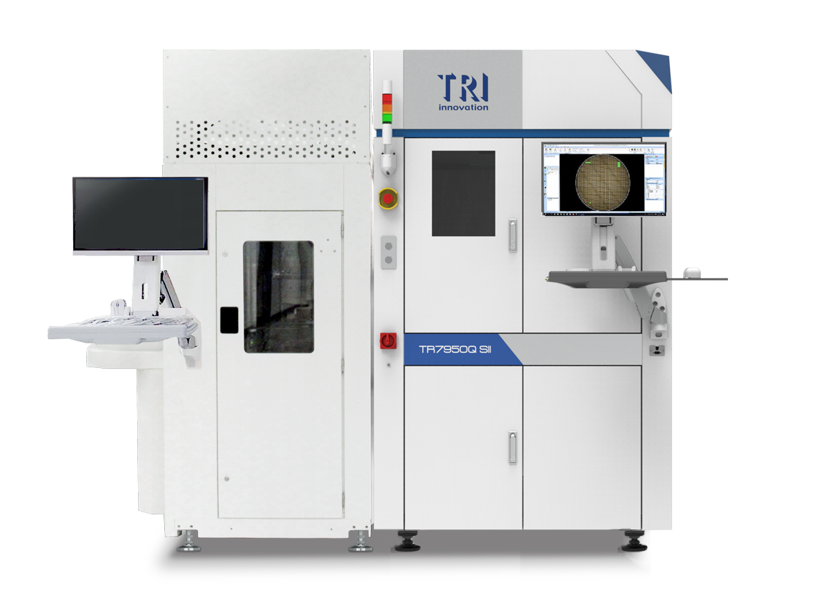
The AI-powered wafer metrology and inspection platform, TR7950Q SII, is built on a high-stability granite platform and the system supports 6“ to 12“ wafers. The platform features robust Automated Visual Inspection (AVI) for high-speed detection of surface defects, including particles, scratches, chipping, contamination, and foreign materials.
The optional Short-Wave Infrared (SWIR) module allows the system to penetrate silicon to detect hidden inner cracks and subsurface defects invisible to standard sensors. For high-detail requirements, the platform offers 0.5 µm or 1 µm high-resolution imaging via the 3D DFF (Depth from Focus) module.
The TR7950Q SII provides high-precision metrology for wafer thickness, top-side warpage, and complex surface topography, alongside high-speed sensing for Through-Silicon Via (TSV) depth, trench dimensions, thin film, and Chiplet metrology.



