
Zum Inhalt springen
EPP Europe
  • News
  • Products
  • Applications
  • Technology
  • Semiconductor
  • Inspection
  • Company News
  • Events
EPP Europe
  • Technology
  • Inspection (AOI/AXI)
  • Semiconductor Packaging
  • Company News
  • Products
  • Trade Shows & Events
    EPP Europe Newsletter
    The most important electronics-manufacturing news delivered to your inbox.

    Info

    • Impressum
    • Datenschutz
    • Barrierefreiheit
    • Datenschutzeinstellungen

    Kontakt zur Redaktion

    EPP EuropeKonradin Mediengruppe
    Ernst-Mey-Str. 8, 70771 Leinfelden-Echterdingen

    E-Mail: redaktion@konradin.de
    Folgen Sie uns
    EPP Europe
    © 2026 EPP Europe
    Startseite/Semiconductor-packaging/Artikel
    Micross to Acquire AEMtec, Strengthening Advanced Packaging Presence in Europe
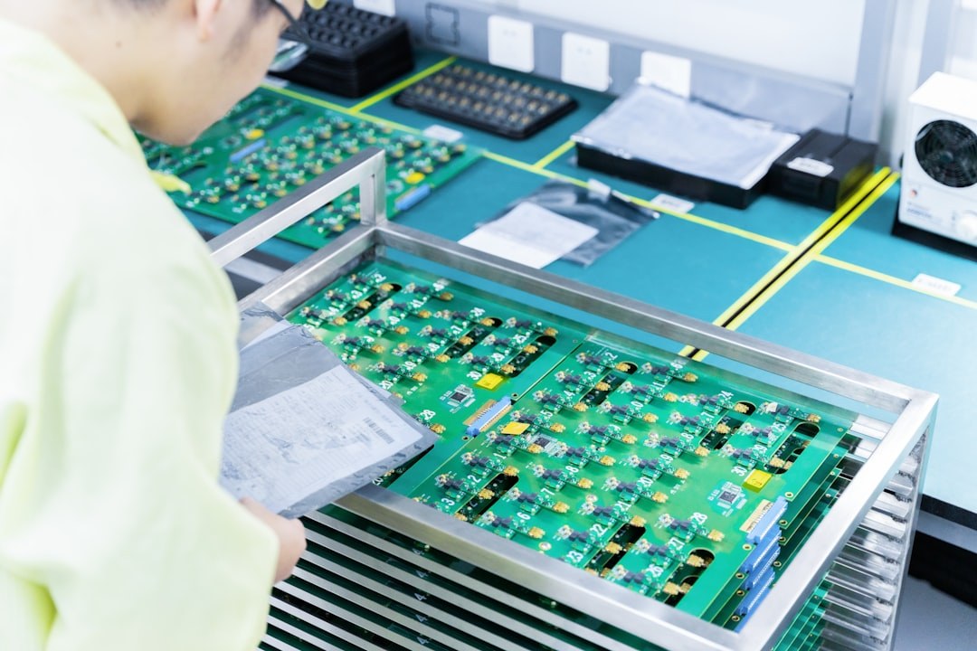
    Foto: Brecht Corbeel / Unsplash
    Semiconductor-packaging

    Micross to Acquire AEMtec, Strengthening Advanced Packaging Presence in Europe

    US-based high-reliability microelectronics provider expands European footprint through acquisition of Berlin-headquartered packaging and optoelectronics specialist
    Veröffentlicht
    15. September 2026
    Lesezeit
    2 Minuten
    Rubrik
    Semiconductor-packaging

    Micross Components, Inc., a US-based provider of high-reliability microelectronic products and services and a portfolio company of Behrman Capital, has announced a definitive agreement to acquire AEMtec GmbH, headquartered in Berlin, Germany. The announcement was made on 28 July 2026 via SEMICON Europa. AEMtec is currently a portfolio company of Capiton.

    AEMtec specialises in complex micro- and optoelectronic module assembly, advanced packaging, and test services for high-reliability applications. The company operates cleanroom facilities in Berlin and Dresden, Germany, as well as in Boston, Massachusetts, USA. Its technology portfolio includes wafer back-end services, wafer testing, chip-on-board (CoB), flip chip assembly, 3D integration, and opto packaging — a breadth of competencies that directly complements Micross' existing service portfolio.

    For the European electronics manufacturing market, the acquisition is notable. AEMtec has established itself as a single-source development and manufacturing partner for demanding customers in the semiconductor, medical and biotechnology, industrial automation, communications, and aerospace and defence sectors. Its end-to-end capability — spanning design, prototyping, industrialisation, qualification, series production and lifecycle support — positions the combined entity as a vertically integrated supplier for complex, mission-critical packaging requirements.

    The deal represents a meaningful consolidation move in the European advanced packaging landscape. Advanced packaging, encompassing heterogeneous integration, 3D stacking and miniaturised optoelectronic assembly, is increasingly relevant as chiplet-based architectures and photonic integration gain traction across industrial and high-reliability markets. AEMtec's existing infrastructure and engineering expertise in these areas gives Micross an established European base from which to serve these growing segments without the lead time of greenfield expansion.

    AEMtec's management team, led by CEO Robert Giertz, will join Micross following completion of the transaction. Financial terms of the agreement have not been disclosed. The acquisition is subject to customary regulatory approvals.

    For European contract manufacturers and OEMs working in high-reliability segments, the transaction signals continued consolidation among specialised packaging service providers. Micross' broader global network — covering high-rel component sourcing, die processing, packaging and test — combined with AEMtec's European cleanroom capacity and optoelectronics know-how, creates a more comprehensive offering for customers requiring qualified, traceable packaging solutions under one roof.

    Quelle: SEMICON Europa – https://www.semi.org/en/node/174011

    Mehr aus Semiconductor-packaging

    Weitere aktuelle Artikel aus der Rubrik Semiconductor-packaging.

    Alle Semiconductor-packaging-Artikel
    Nanoscribe Expands Photoresin Portfolio for Micro-Optics Fabrication via Two-Photon PolymerizationFoto: Brecht Corbeel / Unsplash
    Semiconductor-packaging

    Nanoscribe Expands Photoresin Portfolio for Micro-Optics Fabrication via Two-Photon Polymerization

    11. November 2026

    Nanoscribe has detailed its range of photoresins engineered for Two-Photon Polymerization (2PP) and Two-Photon Grayscale Lithography (2GL), targeting high-precision micro-optics manufacturing on silicon, glass, and…

    Canon Launches FPA-6400ES6a KrF Lithography System with 400 Wafers-per-Hour ThroughputFoto: Canon Europe (semicon)
    Semiconductor-packaging

    Canon Launches FPA-6400ES6a KrF Lithography System with 400 Wafers-per-Hour Throughput

    10. November 2026

    Canon has announced the FPA-6400ES6a KrF scanner for semiconductor lithography, combining a throughput of 400 wafers per hour with industry-leading overlay accuracy of 4.0 nm and the ability to handle wafer warpage of…

    Fabmatics absorbs SCI business activities under unified brandFoto: Ludovico Ceroseis / Unsplash
    Semiconductor-packaging

    Fabmatics absorbs SCI business activities under unified brand

    6. November 2026

    Fabmatics has integrated the business activities of SCI under the Fabmatics brand, consolidating the acquired expertise within its semiconductor automation portfolio.

    Entegris and Kioxia Expand Partnership on Materials Innovation for Next-Gen 3D Flash MemoryFoto: Louis Reed / Unsplash
    Semiconductor-packaging

    Entegris and Kioxia Expand Partnership on Materials Innovation for Next-Gen 3D Flash Memory

    6. November 2026

    Entegris and Kioxia are deepening their strategic partnership to co-develop materials and process technologies for future BiCS FLASH 3D NAND architectures, using AI, digital-twin modelling and experimental validation at…

    ← Zurück zu Semiconductor-packagingZur Startseite


