
Zum Inhalt springen
EPP Europe
  • News
  • Products
  • Applications
  • Technology
  • Semiconductor
  • Inspection
  • Company News
  • Events
EPP Europe
  • Technology
  • Inspection (AOI/AXI)
  • Semiconductor Packaging
  • Company News
  • Products
  • Trade Shows & Events
    EPP Europe Newsletter
    The most important electronics-manufacturing news delivered to your inbox.

    Info

    • Impressum
    • Datenschutz
    • Barrierefreiheit
    • Datenschutzeinstellungen

    Kontakt zur Redaktion

    EPP EuropeKonradin Mediengruppe
    Ernst-Mey-Str. 8, 70771 Leinfelden-Echterdingen

    E-Mail: redaktion@konradin.de
    Folgen Sie uns
    EPP Europe
    © 2026 EPP Europe
    Startseite/Semiconductor-packaging/Artikel
    Mersen to unveil latest SiC power stack reference design
    Bildquelle nicht angegeben
    Semiconductor-packaging

    Mersen to unveil latest SiC power stack reference design

    Mersen, a leader in the field of electrical protection and power management solutions, will present a diversity of new products and solutions for power
    Veröffentlicht
    02. Mai 2024
    Lesezeit
    2 Minuten
    Rubrik
    Semiconductor-packaging

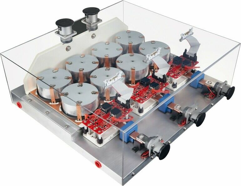
    Latest SiC Power Stack reference design.

    The company will introduce its latest SiC Power Stack reference design. With capabilities up to 1200 Vdc DC bus and up to 300 Arms at 25 kHz, this evaluation kit helps inverter designers save time and confusion in selecting individual components by taking benefit from a solution that is optimally pre-designed for their specific application (e.g. DC Smart Grid, EV charging stations, renewables, e-mobility). In addition, Mersen unique capacitor-to-bus-bar assembly technique offers DC-link inductance as low as 7 nH.

    DC high voltage fuses for 1500 V, 1000 V and 500 V platforms

    At PCIM, the company will also present innovative products for emerging markets. The focus will be on new fuses for energy storage systems, charging stations and electric vehicles. With ABAT and GBAT fuses for energy storage, D-fuses for charging stations and MEV fuses for electric vehicles, Mersen has developed a complete product portfolio to withstand high alternating load cycles and low power losses, which improves the reliability and efficiency of the system. The new Power Pack fuse design will be introduced during PCIM. The power pack fuse proof of concept has been specifically designed to meet the latest MegaWatt Charging requirements.

    Custom solutions for cooling, bus bars and capacitors

    Visitors to PCIM can also learn about Mersen’s expertise in a wide range of passive components like cooling plates, capacitors and bus bars solutions.

    The company has extensive expertise in vacuum brazing and in the simulation of cooling systems for power electronic components, as well as in 180 °C high temperature and very low inductance bus bars. Mersen also has decades of experience in the production of custom capacitor solutions and their sub-assembly with bus bars.

    Live presentation on electric vehicles

    In addition to numerous products, visitors to the booth can look forward to an exciting presentation on new challenges in EV battery protection and interconnection on June 11 and 12 from 12:30 to 12:50.

    Furthermore, VP Power Stack Product Line Philippe Roussel will be available every day on the booth to present the latest developments from Mersen in Power Stack optimization.

    PCIM Europe: Hall 9, Stand 534

    Mehr aus Semiconductor-packaging

    Weitere aktuelle Artikel aus der Rubrik Semiconductor-packaging.

    Alle Semiconductor-packaging-Artikel
    Nanoscribe Expands Photoresin Portfolio for Micro-Optics Fabrication via Two-Photon PolymerizationFoto: Brecht Corbeel / Unsplash
    Semiconductor-packaging

    Nanoscribe Expands Photoresin Portfolio for Micro-Optics Fabrication via Two-Photon Polymerization

    11. November 2026

    Nanoscribe has detailed its range of photoresins engineered for Two-Photon Polymerization (2PP) and Two-Photon Grayscale Lithography (2GL), targeting high-precision micro-optics manufacturing on silicon, glass, and…

    Canon Launches FPA-6400ES6a KrF Lithography System with 400 Wafers-per-Hour ThroughputFoto: Canon Europe (semicon)
    Semiconductor-packaging

    Canon Launches FPA-6400ES6a KrF Lithography System with 400 Wafers-per-Hour Throughput

    10. November 2026

    Canon has announced the FPA-6400ES6a KrF scanner for semiconductor lithography, combining a throughput of 400 wafers per hour with industry-leading overlay accuracy of 4.0 nm and the ability to handle wafer warpage of…

    Fabmatics absorbs SCI business activities under unified brandFoto: Ludovico Ceroseis / Unsplash
    Semiconductor-packaging

    Fabmatics absorbs SCI business activities under unified brand

    6. November 2026

    Fabmatics has integrated the business activities of SCI under the Fabmatics brand, consolidating the acquired expertise within its semiconductor automation portfolio.

    Entegris and Kioxia Expand Partnership on Materials Innovation for Next-Gen 3D Flash MemoryFoto: Louis Reed / Unsplash
    Semiconductor-packaging

    Entegris and Kioxia Expand Partnership on Materials Innovation for Next-Gen 3D Flash Memory

    6. November 2026

    Entegris and Kioxia are deepening their strategic partnership to co-develop materials and process technologies for future BiCS FLASH 3D NAND architectures, using AI, digital-twin modelling and experimental validation at…

    ← Zurück zu Semiconductor-packagingZur Startseite


