
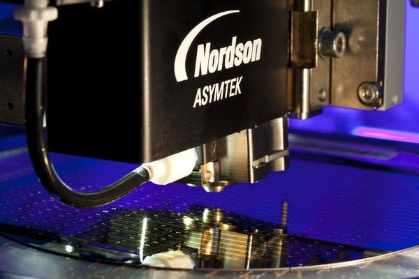
Mr. Morita will explain the structure of the 3D package, the two types of underfill required by this package structure, along with the technologies used to apply the underfill. These packages have very tight bump pitch and height between the stacked die which make the conventional underfill processes, like capillary and molded, difficult. In addition, chip-on-wafer stacking needs very tight die placement between side-by-side dies, making it hard for underfill to penetrate through the tight die placement after bonding. As a result, pre-applied underfill is gaining attention. The presentation „Wafer Spray Coating for Pre-applied Underfill“ addresses pre-applied underfill challenges and requirements, coating technology options and comparisons, and the best apparatus to use for completing the underfill process. Using experience gained from conformal coating and jet dispensing has enabled development of a process of wafer spray coating for pre-applied underfill application because it can address the thickness consistency and material wastage challenges. The International Wafer-Level Packaging Conference (IWLPC) brings together some of the semiconductor industry’s most respected authorities addressing all aspects of wafer-level, 3D, TSV, and MEMS device packaging.



