
Zum Inhalt springen
EPP Europe
  • News
  • Products
  • Applications
  • Technology
  • Semiconductor
  • Inspection
  • Company News
  • Events
EPP Europe
  • Technology
  • Inspection (AOI/AXI)
  • Semiconductor Packaging
  • Company News
  • Products
  • Trade Shows & Events
    EPP Europe Newsletter
    The most important electronics-manufacturing news delivered to your inbox.

    Info

    • Impressum
    • Datenschutz
    • Barrierefreiheit
    • Datenschutzeinstellungen

    Kontakt zur Redaktion

    EPP EuropeKonradin Mediengruppe
    Ernst-Mey-Str. 8, 70771 Leinfelden-Echterdingen

    E-Mail: redaktion@konradin.de
    Folgen Sie uns
    EPP Europe
    © 2026 EPP Europe
    Startseite/Semiconductor-packaging/Artikel
    Maximum Printing Precision For Your Semiconductor & Hybrid Applications
    Bildquelle nicht angegeben
    Semiconductor-packaging

    Maximum Printing Precision For Your Semiconductor & Hybrid Applications

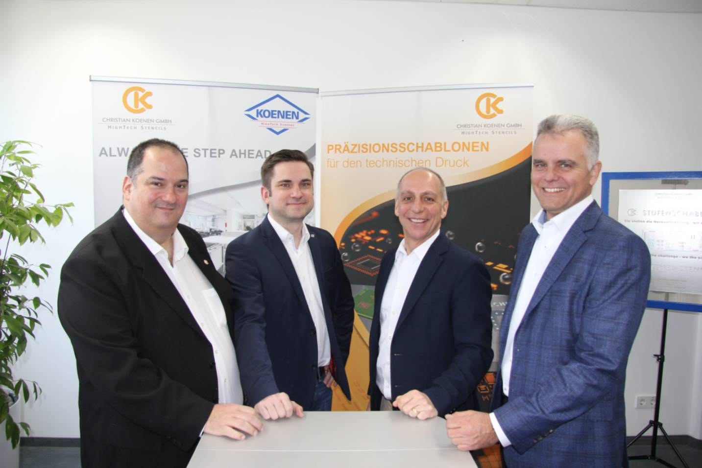
    The CK Group is focused on the screen and stencil printing process. They manufacture precision tools for electronics manufacturing.
    Veröffentlicht
    11. März 2022
    Lesezeit
    2 Minuten
    Rubrik
    Semiconductor-packaging

    Many of our precision stencils are used in manufacturing processes with print deposits smaller than 30µm. This high accuracy with accompanying process reliability enables applications in semiconductor manufacturing.

    Due to the advancing miniaturization of SMD components and the increasing mix of components on ever smaller surfaces, the demands on material application are constantly increasing. The CK Group is focused on the screen and stencil printing process. We manufacture precision tools for electronics manufacturing in short delivery times. With our Application Centre we have been investing in process consulting, process analysis, production testing and printing process optimization for many years.

    With innovative production technologies and experienced employees at the locations Munich, Eisleben, Györ (HU) and Le Longeron (FR), more than 75,000 precision tools (screens and stencils) are produced every year. Our state of the art manufacturing technologies are exceeding the usual market quality requirements in terms of accuracy and speed.

    Semicon Application Areas

    Artikelbild
    Source: CK Group

    Wafer Bumping Stencils

    In wafer bumping, it is important that the solder paste is optimally transferred from the stencil. Uniform paste deposits are the requirement for a reproducible bump height. Our laser-cut wafer bumping stencils meet the highest demands in combination with innovative materials such as CK Nanovate™ Nickel. They are extremely thin and densely packed with the smallest apertures.

    Product features – Maximum precision for your semiconductors

    • Reproducible bump formation due to superalloys with smooth cutting surfaces
    • More print cycles due to long stencil life
    • Higher efficiency and productivity of the wafer bumping process

    LTCC Stencils

    In the production of circuit carriers based on ceramics (low-temperature cofired ceramics), circuit levels must be reliably plated through.
    Our laser-cut LTCC stencils (VIA fill stencils) have super-fine apertures that are placed precisely on the micro-VIAs of the ceramic substrate. When the silver paste is applied to the stencil, the apertures guide it into the VIAs like a funnel. Play it safe with the VIA Fill process and decide for precise connections and minimal deviations along the tolerance chain. And that with apertures from 50µm and a positional accuracy of ± 10µm.

    Product features – Maximum precision for hybrid technologies

    • Precise aperture positioning due to superalloy CK Nanovate™ Nickel
    • More print cycles due to long stencil life
    • Higher economic efficiency and productivity of the VIA fill process

    CK Balling Stencil

    Artikelbild
    Source: CK Group

    The production of semiconductors places the highest demands on efficiency. Do you want to apply flipchip bumps to wafers or substrates as efficiently as possible? With CK Balling stencils, you can raise the productivity of your semiconductor production to a new level. The secret: With our patented milling process, we also add the necessary spacers to the lasered apertures.

    This time-saving process brings you two important advantages: Positionally accurate apertures and short delivery times.

    Product features – Precise apertures and exact positioning

    • High precision and reproducibility for apertures and spacers
    • Shorter delivery times compared to electroformed stencils
    • Optional process evaluation in the CK Application Center

    Mehr aus Semiconductor-packaging

    Weitere aktuelle Artikel aus der Rubrik Semiconductor-packaging.

    Alle Semiconductor-packaging-Artikel
    Nanoscribe Expands Photoresin Portfolio for Micro-Optics Fabrication via Two-Photon PolymerizationFoto: Brecht Corbeel / Unsplash
    Semiconductor-packaging

    Nanoscribe Expands Photoresin Portfolio for Micro-Optics Fabrication via Two-Photon Polymerization

    11. November 2026

    Nanoscribe has detailed its range of photoresins engineered for Two-Photon Polymerization (2PP) and Two-Photon Grayscale Lithography (2GL), targeting high-precision micro-optics manufacturing on silicon, glass, and…

    Canon Launches FPA-6400ES6a KrF Lithography System with 400 Wafers-per-Hour ThroughputFoto: Canon Europe (semicon)
    Semiconductor-packaging

    Canon Launches FPA-6400ES6a KrF Lithography System with 400 Wafers-per-Hour Throughput

    10. November 2026

    Canon has announced the FPA-6400ES6a KrF scanner for semiconductor lithography, combining a throughput of 400 wafers per hour with industry-leading overlay accuracy of 4.0 nm and the ability to handle wafer warpage of…

    Fabmatics absorbs SCI business activities under unified brandFoto: Ludovico Ceroseis / Unsplash
    Semiconductor-packaging

    Fabmatics absorbs SCI business activities under unified brand

    6. November 2026

    Fabmatics has integrated the business activities of SCI under the Fabmatics brand, consolidating the acquired expertise within its semiconductor automation portfolio.

    Entegris and Kioxia Expand Partnership on Materials Innovation for Next-Gen 3D Flash MemoryFoto: Louis Reed / Unsplash
    Semiconductor-packaging

    Entegris and Kioxia Expand Partnership on Materials Innovation for Next-Gen 3D Flash Memory

    6. November 2026

    Entegris and Kioxia are deepening their strategic partnership to co-develop materials and process technologies for future BiCS FLASH 3D NAND architectures, using AI, digital-twin modelling and experimental validation at…

    ← Zurück zu Semiconductor-packagingZur Startseite


