
Zum Inhalt springen
EPP Europe
  • News
  • Products
  • Applications
  • Technology
  • Semiconductor
  • Inspection
  • Company News
  • Events
EPP Europe
  • Technology
  • Inspection (AOI/AXI)
  • Semiconductor Packaging
  • Company News
  • Products
  • Trade Shows & Events
    EPP Europe Newsletter
    The most important electronics-manufacturing news delivered to your inbox.

    Info

    • Impressum
    • Datenschutz
    • Barrierefreiheit
    • Datenschutzeinstellungen

    Kontakt zur Redaktion

    EPP EuropeKonradin Mediengruppe
    Ernst-Mey-Str. 8, 70771 Leinfelden-Echterdingen

    E-Mail: redaktion@konradin.de
    Folgen Sie uns
    EPP Europe
    © 2026 EPP Europe
    Startseite/Semiconductor-packaging/Artikel
    Leadframe Marking
    Bildquelle nicht angegeben
    Semiconductor-packaging

    Leadframe Marking

    Intro A lead frame is the metal structure inside a chip package that carries signals from the die to the outside. It is usually formed from a copper
    Veröffentlicht
    10. Juni 2022
    Lesezeit
    2 Minuten
    Rubrik
    Semiconductor-packaging

    Intro

    A lead frame is the metal structure inside a chip package that carries signals from the die to the outside. It is usually formed from a copper strip. It may be treated by a plated finish to prevent the copper from oxidation. Depending on the metal surface different lasers are used to form a direct laser marking to achieve a permanent marking for traceability in semiconductor packaging.

    No need for consumables and the speed of processing lead to the low COO of the laser marking process.

    Laser Marking Physics

    Common available laser technologies start from the long wavelength IR low power CO2 lasers at 10.600 nm through NIR DPSS laser or fiber lasers at 1064 nm to DPSS lasers with SHG at 532 nm or THG at 355 nm.

    Converting DPSS lasers from the fundamental NIR wavelength to VIS green or UV is often called frequency doubling or tripling.

    The beam steering in laser systems is common for all useful wavelengths. So-called Galvo Scanners use galvanometric beam deflection by mirrors to position the laser beam very fast and precise. Appropriate f-theta lenses and beam expanders allow for the right laser spot size and working area in XY commonly called scan field.

    The type of laser beam sources used for marking are process specific. Lasers in IR show almost no absorption in leadframe metals and are useless therefore as almost 100 % of the laser radiation is being reflected.

    Absorption of NIR laser radiation at 1064 nm is low in bare polished copper at room temperature and increases with temperature. This effect allows to use specific fiber lasers with adapted pulse lengths for marking copper.

    Fiber lasers are well established in electronic industries due to their ease of integration and low maintenance and come at an attractive price. Especially MOPA fiber lasers with their wide range of laser parameters including pulse length can be used effectively for laser marking applications.

    Using 532 nm green lasers for marking benefits from the higher absorption in copper. In addition, the shorter wavelength allows for smaller spot sizes.

    Blue 450 nm diode lasers are recently available at attractive cost and allow for even better absorption in copper due to their shorter wavelength.

    The aforementioned plating may help to create a good contrast and enhances machine readability.

    These markings can be realized by the ASYS product line POLYPHOS MK, which is capable of laser marking metal and polymer surfaces.

    Picture 4: Absorption spectrum of different metals
    Picture 4: Absorption spectrum of different metals

    Results

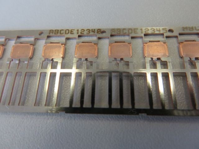
    Picture 1 shows a laser mark on a tin plated TO-220 transistor leadframe by fiber laser. The following pictures are showing the results of laser marking on leadframes:

    Picture 5: Microscopic view of picture 1 (TO-220 package leadframe)
    Picture 5: Microscopic view of picture 1 (TO-220 package leadframe)
    Picture 6: DMC on TO-220 leadframe
    Picture 6: DMC on TO-220 leadframe
    Picture 7: DMC on picture 3 leadframe by fiber laser
    Picture 7: DMC on picture 3 leadframe by fiber laser
    Picture 8: Optical bench for laser optics
    Picture 8: Optical bench for laser optics

    Mehr aus Semiconductor-packaging

    Weitere aktuelle Artikel aus der Rubrik Semiconductor-packaging.

    Alle Semiconductor-packaging-Artikel
    Nanoscribe Expands Photoresin Portfolio for Micro-Optics Fabrication via Two-Photon PolymerizationFoto: Brecht Corbeel / Unsplash
    Semiconductor-packaging

    Nanoscribe Expands Photoresin Portfolio for Micro-Optics Fabrication via Two-Photon Polymerization

    11. November 2026

    Nanoscribe has detailed its range of photoresins engineered for Two-Photon Polymerization (2PP) and Two-Photon Grayscale Lithography (2GL), targeting high-precision micro-optics manufacturing on silicon, glass, and…

    Canon Launches FPA-6400ES6a KrF Lithography System with 400 Wafers-per-Hour ThroughputFoto: Canon Europe (semicon)
    Semiconductor-packaging

    Canon Launches FPA-6400ES6a KrF Lithography System with 400 Wafers-per-Hour Throughput

    10. November 2026

    Canon has announced the FPA-6400ES6a KrF scanner for semiconductor lithography, combining a throughput of 400 wafers per hour with industry-leading overlay accuracy of 4.0 nm and the ability to handle wafer warpage of…

    Fabmatics absorbs SCI business activities under unified brandFoto: Ludovico Ceroseis / Unsplash
    Semiconductor-packaging

    Fabmatics absorbs SCI business activities under unified brand

    6. November 2026

    Fabmatics has integrated the business activities of SCI under the Fabmatics brand, consolidating the acquired expertise within its semiconductor automation portfolio.

    Entegris and Kioxia Expand Partnership on Materials Innovation for Next-Gen 3D Flash MemoryFoto: Louis Reed / Unsplash
    Semiconductor-packaging

    Entegris and Kioxia Expand Partnership on Materials Innovation for Next-Gen 3D Flash Memory

    6. November 2026

    Entegris and Kioxia are deepening their strategic partnership to co-develop materials and process technologies for future BiCS FLASH 3D NAND architectures, using AI, digital-twin modelling and experimental validation at…

    ← Zurück zu Semiconductor-packagingZur Startseite



