
Zum Inhalt springen
EPP Europe
  • News
  • Products
  • Applications
  • Technology
  • Semiconductor
  • Inspection
  • Company News
  • Events
EPP Europe
  • Technology
  • Inspection (AOI/AXI)
  • Semiconductor Packaging
  • Company News
  • Products
  • Trade Shows & Events
    EPP Europe Newsletter
    The most important electronics-manufacturing news delivered to your inbox.

    Info

    • Impressum
    • Datenschutz
    • Barrierefreiheit
    • Datenschutzeinstellungen

    Kontakt zur Redaktion

    EPP EuropeKonradin Mediengruppe
    Ernst-Mey-Str. 8, 70771 Leinfelden-Echterdingen

    E-Mail: redaktion@konradin.de
    Folgen Sie uns
    EPP Europe
    © 2026 EPP Europe
    Startseite/Semiconductor-packaging/Artikel
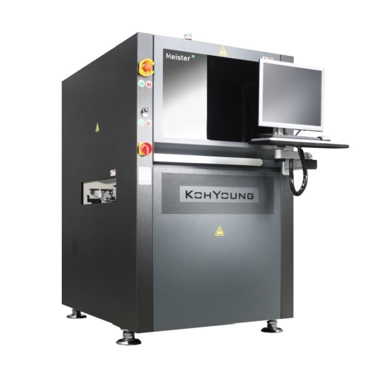
    Koh Young Launches the Meister D+ for Semiconductor Package Inspection
    Bildquelle nicht angegeben
    Semiconductor-packaging

    Koh Young Launches the Meister D+ for Semiconductor Package Inspection

    Koh Young, industry leader in True3D™ measurement-based inspection solutions, announces the release of its new Meister D+.
    Veröffentlicht
    05. März 2022
    Lesezeit
    2 Minuten
    Rubrik
    Semiconductor-packaging

    Koh Young, the industry leader in True3D™ measurement-based inspection solutions, announces the release of its new Meister D+ semiconductor inspection solution. Premium True3D™ Inspection Solution for Chiplets and System-in-Package (SiP) devices including die and surface mount components. The new Meister D+ is an extension of the Meister product family that features solutions ranging from solder paste, printed bumps, and solder ball to small components like 0201Ms and highly reflective die.

    Meister D+: Industry Leading Inspection Systems for Advanced Packaging and Semiconductor Applications

    As advanced packages continue evolving, device thickness is paramount since consumers demand smaller products with more functionality. As such, the die must be thinned, which creates a mirror-like surface that challenges optical inspection due to its highly reflective surface. Additionally, tight interspacing and increasing aspect ratios further complicate inspection. Yet, as the name implies, the Meister D+ dominants these challenges with industry leading True3D measurement accuracy and inspection technologies.

    The latest Meister D+ system is perfected for component and die inspection, while delivering fast, accurate inspection from an 8-projector probe. It targets MCM/SiP/Chiplet inspection with integrated measurement and defect analysis software built on a proprietary AI engine. Beyond 0201M (008004) microchips, 10um bump height, and 5um gap spacing, it detects die defects like micro-cracks, chippings, and foreign material with high accuracy/repeatability. Additionally, this 3D solution supports a wide range of inspection capabilities: missing, offset, rotation, polarity, dimension, co-planarity, and more.

    With its Moiré technology, new 12MegaPixel/5-micron optics, and 300mm^2/second inspection speed, the Meister D+ is the first solution for production-speed 3D inspection for modules combining microchips and mirror-finish die. With its userfriendly GUI and programming wizards, it virtually eliminates fine-tuning and teaching, which quickens the production ramp. Plus, its IPC-CFX-2591, IPC-HERMES-9852, and IPC-DPMX-2581 compatibility makes connectivity simple and secure.

    With innovative technologies, Meister D+ delivers best-in-class performance and functionality. Its inspection capabilities have already been qualified for mass production by major semiconductor companies throughout the world. The recognized leader in electronics measurement and inspection, Koh Young continues to deliver solutions for the electronics manufacturing industry.


    Mehr aus Semiconductor-packaging

    Weitere aktuelle Artikel aus der Rubrik Semiconductor-packaging.

    Alle Semiconductor-packaging-Artikel
    Nanoscribe Expands Photoresin Portfolio for Micro-Optics Fabrication via Two-Photon PolymerizationFoto: Brecht Corbeel / Unsplash
    Semiconductor-packaging

    Nanoscribe Expands Photoresin Portfolio for Micro-Optics Fabrication via Two-Photon Polymerization

    11. November 2026

    Nanoscribe has detailed its range of photoresins engineered for Two-Photon Polymerization (2PP) and Two-Photon Grayscale Lithography (2GL), targeting high-precision micro-optics manufacturing on silicon, glass, and…

    Canon Launches FPA-6400ES6a KrF Lithography System with 400 Wafers-per-Hour ThroughputFoto: Canon Europe (semicon)
    Semiconductor-packaging

    Canon Launches FPA-6400ES6a KrF Lithography System with 400 Wafers-per-Hour Throughput

    10. November 2026

    Canon has announced the FPA-6400ES6a KrF scanner for semiconductor lithography, combining a throughput of 400 wafers per hour with industry-leading overlay accuracy of 4.0 nm and the ability to handle wafer warpage of…

    Fabmatics absorbs SCI business activities under unified brandFoto: Ludovico Ceroseis / Unsplash
    Semiconductor-packaging

    Fabmatics absorbs SCI business activities under unified brand

    6. November 2026

    Fabmatics has integrated the business activities of SCI under the Fabmatics brand, consolidating the acquired expertise within its semiconductor automation portfolio.

    Entegris and Kioxia Expand Partnership on Materials Innovation for Next-Gen 3D Flash MemoryFoto: Louis Reed / Unsplash
    Semiconductor-packaging

    Entegris and Kioxia Expand Partnership on Materials Innovation for Next-Gen 3D Flash Memory

    6. November 2026

    Entegris and Kioxia are deepening their strategic partnership to co-develop materials and process technologies for future BiCS FLASH 3D NAND architectures, using AI, digital-twin modelling and experimental validation at…

    ← Zurück zu Semiconductor-packagingZur Startseite

