
Zum Inhalt springen
EPP Europe
  • News
  • Products
  • Applications
  • Technology
  • Semiconductor
  • Inspection
  • Company News
  • Events
EPP Europe
  • Technology
  • Inspection (AOI/AXI)
  • Semiconductor Packaging
  • Company News
  • Products
  • Trade Shows & Events
    EPP Europe Newsletter
    The most important electronics-manufacturing news delivered to your inbox.

    Info

    • Impressum
    • Datenschutz
    • Barrierefreiheit
    • Datenschutzeinstellungen

    Kontakt zur Redaktion

    EPP EuropeKonradin Mediengruppe
    Ernst-Mey-Str. 8, 70771 Leinfelden-Echterdingen

    E-Mail: redaktion@konradin.de
    Folgen Sie uns
    EPP Europe
    © 2026 EPP Europe
    Startseite/Semiconductor-packaging/Artikel
    Junkosha Introduces 1 mm Pitch High-Flex Cable for Semiconductor Vacuum Equipment
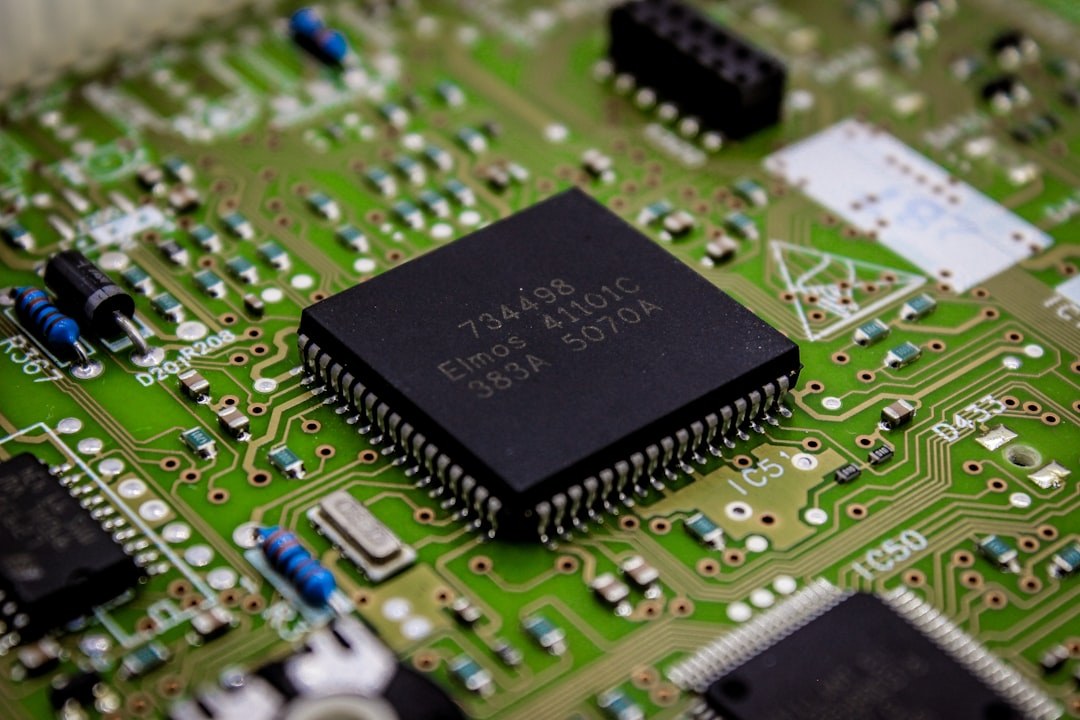
    Foto: Yogesh Phuyal / Unsplash
    Semiconductor-packaging

    Junkosha Introduces 1 mm Pitch High-Flex Cable for Semiconductor Vacuum Equipment

    Super Low Outgassing Cable targets space-constrained motion applications in ultra-high vacuum chambers with 30 million cycle flex life
    Veröffentlicht
    20. Oktober 2026
    Lesezeit
    2 Minuten
    Rubrik
    Semiconductor-packaging

    Junkosha, a specialist in advanced cable solutions for semiconductor manufacturing equipment, has announced a new 1 mm pitch configuration within its Junkosha Super Low Outgassing Cable portfolio. The announcement was made at SEMICON West 2026, where the company used the event to highlight its collaborative cable engineering approach with semiconductor equipment manufacturers (SEMs).

    The new cable configuration addresses a persistent integration challenge in semiconductor equipment design: space constraints within ultra-high vacuum (UHV) chambers. In environments where linear stages, motors, and encoders are already tightly packaged, even a marginal increase in cable width can force redesigns of routing arrangements, mechanical interfaces, or assembly tooling. The 1 mm pitch configuration is intended to minimise such downstream engineering impact.

    According to Junkosha, the cables have achieved a flex life of 30 million cycles at a 70 mm bending radius, qualifying them for demanding high-flex motion applications typical of vacuum-compatible linear and rotary stage assemblies. Low outgassing performance is a critical requirement in UHV environments, where volatile compounds released from materials can contaminate process chambers and compromise yield in wafer-level processes.

    The product development follows what Junkosha describes as a collaborative engineering model, working directly with equipment manufacturers to define, test, and refine cable geometries and material specifications around application-specific requirements rather than adapting standard catalogue products. This approach is increasingly relevant as semiconductor equipment architectures become more compact and the tolerance for integration compromise narrows.

    For the European electronics manufacturing supply chain, cable qualification for semiconductor equipment is a discipline that intersects with broader advanced packaging and wafer handling trends. As front-end equipment suppliers face pressure to reduce equipment footprints while maintaining throughput and reliability, subsystem components including cabling must meet tighter dimensional and performance specifications.

    Junkosha's Super Low Outgassing Cable portfolio is positioned for integration into equipment used across etch, deposition, lithography, and inspection segments, where vacuum-compatible, high-cycle-life interconnects are standard requirements. The 1 mm pitch variant extends the range to applications where previous configurations were dimensionally impractical.

    Quelle: SEMICON Europa – https://www.semi.org/en/node/176426

    Mehr aus Semiconductor-packaging

    Weitere aktuelle Artikel aus der Rubrik Semiconductor-packaging.

    Alle Semiconductor-packaging-Artikel
    Nanoscribe Expands Photoresin Portfolio for Micro-Optics Fabrication via Two-Photon PolymerizationFoto: Brecht Corbeel / Unsplash
    Semiconductor-packaging

    Nanoscribe Expands Photoresin Portfolio for Micro-Optics Fabrication via Two-Photon Polymerization

    11. November 2026

    Nanoscribe has detailed its range of photoresins engineered for Two-Photon Polymerization (2PP) and Two-Photon Grayscale Lithography (2GL), targeting high-precision micro-optics manufacturing on silicon, glass, and…

    Canon Launches FPA-6400ES6a KrF Lithography System with 400 Wafers-per-Hour ThroughputFoto: Canon Europe (semicon)
    Semiconductor-packaging

    Canon Launches FPA-6400ES6a KrF Lithography System with 400 Wafers-per-Hour Throughput

    10. November 2026

    Canon has announced the FPA-6400ES6a KrF scanner for semiconductor lithography, combining a throughput of 400 wafers per hour with industry-leading overlay accuracy of 4.0 nm and the ability to handle wafer warpage of…

    Fabmatics absorbs SCI business activities under unified brandFoto: Ludovico Ceroseis / Unsplash
    Semiconductor-packaging

    Fabmatics absorbs SCI business activities under unified brand

    6. November 2026

    Fabmatics has integrated the business activities of SCI under the Fabmatics brand, consolidating the acquired expertise within its semiconductor automation portfolio.

    Entegris and Kioxia Expand Partnership on Materials Innovation for Next-Gen 3D Flash MemoryFoto: Louis Reed / Unsplash
    Semiconductor-packaging

    Entegris and Kioxia Expand Partnership on Materials Innovation for Next-Gen 3D Flash Memory

    6. November 2026

    Entegris and Kioxia are deepening their strategic partnership to co-develop materials and process technologies for future BiCS FLASH 3D NAND architectures, using AI, digital-twin modelling and experimental validation at…

    ← Zurück zu Semiconductor-packagingZur Startseite


