
Having the theme “Heterogenous Integration: Bolstering Europe’s Resilience”, the summit and exhibition aims to unravel the latest breakthroughs driving innovation in chiplet architectures, hybrid bonding, photonics and advanced system-level design. From geopolitical dynamics to chiplet applications and hybrid bonding techniques, attendees will dive deep into the critical role of 3D and heterogeneous integration in strengthening Europe’s semiconductor value chain.
„SEMI Europe looks forward to welcoming global advanced packaging experts to Dresden,” commented Laith Altimime, President of SEMI Europe. “With an exceptional speaker lineup and a sold-out exhibition, the summit will spotlight critical advancements in chiplet technologies, hybrid bonding, and photonics; all [of which are] essential for enabling next-generation intelligent systems and bolstering Europe’s technological resilience.”
The topics will include:
- Geopolitical dynamics and market trends in a global semiconductor landscape;
- chiplet applications and system-level architectures;
- hybrid bonding technologies for die-to-wafer and wafer-to-wafer integration;
- photonics and co-packaged optics;
- innovation and sustainability in 3D integration; and
- European readiness in design, materials, and manufacturing.
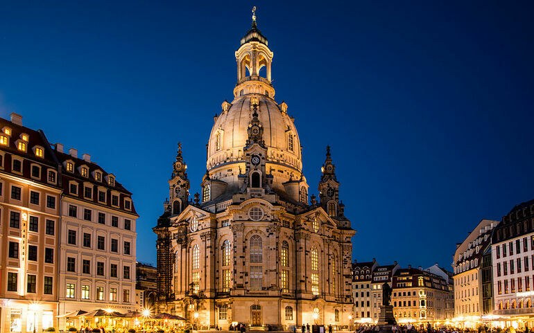
See the event website for a list of featured speakers. This year’s networking reception will take place at the Hilton Dresden Hotel on the first day of the event. A networking dinner cruise will take summit attendees on a historic paddle steamer on the Elbe River.
The summit exhibition is set to feature prominent names in 3D integration microelectronics manufacturing, who will showcase their latest products and technologies.



