
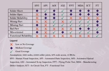
No single test technique is a ”cure-all” for all challenges; each has its own strengths and weaknesses and needs to be evaluated as a possible solution within the overall test plan. Although automated inspection methods are capable of finding defects closer to the source for quick debug and repair, they do not ensure confidence in product function, as do ICT and functional test methods. Utilizing a distributed test approach with the optimum level of complementary and overlapping fault coverage will deliver the quality levels and production efficiencies dictated by the application, and will characterize a successful strategy. A distributed approach can address the right balance of competing factors like diagnostic resolution, fault coverage, test access, test development time, skill levels and training costs, uptime and utilization, cost and throughput.
How do we develop best-practice distributed test strategies? Since each test approach has varying performance levels along many different measurement characteristics (fault coverage table figure 1), we can imagine the evaluation matrix growing to unmanageable proportions. When solving a problem with such a complexity, a software analysis approach is required. Without an effective quantitative approach, the high number of choices and convoluted, overlapping characteristics of the different test methods would make optimizing a test strategy very difficult and time consuming and lead to questionable results at best.
ICT combined with human visual inspection has been an effective test strategy for many years and has been arbitrarily applied to many PCBAs without analysis. But board assemblies in cost and time-competitive environment require that we achieve a more optimal test performance for each board on a case-by-case basis. This requires software modeling of test coverage for specific component reference designator pins in order to address issues of lost ICT access, fault coverage of library device models and the particular performance requirements of individual boards. This type of comprehensive analysis can only be performed with a tool that takes into account all board information. The standardization of data sets has allowed software tools to emerge and solve analysis problems by linking product and process technology with test capability. Each PCBA will reveal a unique fault spectrum. If the software is used to design a test strategy with the fault spectrum of the board, a more optimum and complete result will be achieved. A critical requirement for boards with limited ICT access is testability analysis during design. Optimization and modeling software that enables testability analysis prior to the PCB layout routing will deliver fewer design iterations, faster time-to-market, improved fault coverage and lower production test costs.
The slowdown in the industry has led to increased focus on cost and efficiency. Declining revenues and overcapacity has created an environment where manufacturers are hesitant to invest in technology and capital equipment. Test optimization software can help through this period by performing what-if scenarios to better leverage existing capital infrastructure in a distributed test approach to achieve more optimal manufacturing performance levels.
The optimization software for managing the distributed test and inspection environment, Strategist of Teradyne/GenRad, gives users the capability to develop multiple test strategies that maximize fault coverage and inspection efficiencies, while improving time-to-market and time-to-volume. Best-practice test strategies are developed to ensure that modeling the fault spectrum and pin-level fault coverage of each test method optimizes fault coverage and throughput. The software analyzes the design of a board, models the production line configuration, and optimizes the test and inspection strategies based on actual line layout. It eliminates manual test distribution, saving hours of work per board. The open, vendor-neutral software architecture supports programming for 2D/3D X-ray, AOI, ICT/FT and manufacturing defect analyzers. The tool addresses the challenge of manufacturing complex PCBAs which have limited physical test access. And it accelerates manufacturers’ goals of improving time-to-market, time-to-volume and time-to-profit by facilitating concurrent engineering to optimize verification concepts prior to manufacturing.
DFx is a key focus area because it accelerates time-to-market and time-to-volume, reduces manufacturing costs and lowers defect rates. By verifying PCB designs with a rules checker, non-conformances that could severely affect production-quality levels can be rectified. Similarly, effective testability analysis during design can significantly improve production test performance. Strategist enables test engineers to work concurrently with designers, to predict fault spectrum, plan test strategies, understand fault coverage and test-access tradeoffs prior to the layout routing. Because the tool calculates a fault spectrum for every pin, component and signal on the board, it can identify which test pads will provide the greatest test coverage. By listing these test pads in descending order, designers can make intelligent decisions on which pads should be provided on boards with limited access. The bottom line is fewer design iterations, fewer snags and improved test performance at lower cost. Because the tool models the fault coverage provided by each machine in the test plan, it can identify which test pads can be removed due to overlapping coverage.
Strategist uses analog, digital and boundary-scan model libraries for accurate analysis of ICT, MDA and FPT test coverage. All component models are stored in an open-architecture, non-vendor specific library format. This neutral format can be automatically generated using available tools that will translate vendor-specific models into the neutral format. Users can update component models within the library and import other types as well. The library models provide pin-function and device-structure information that allows intelligent decisions regarding ICT access requirements for multi-unit analog and digital devices. This would include, for example, identification of individual resistors within a resistor pack to provide single unit tests. Strategist will also identify BS nets and their test access ports (TAP) for probe removal techniques. The digital model includes the pins required for test, isolation and bus diagnostics, but does not include the test vectors.
Different factors constrain test strategies on boards that serve different requirements. Sometimes the constraining factor is access in which case Strategist can be used to deliver a complementary test approach between ICT and AXI for example, which could be – as we can see – executed in two ways.
Full AXI complemented with ICT – this strategy achieves maximum probe and test-pad reduction because it assumes that shorts and opens will be tested on each pin by AXI, and furthermore that overlapping shorts/opens coverage on these same pins is not required at ICT. With this methodology, ICT is used only to verify that a functional part of the correct value has been placed at the location. This can be achieved by testing only one unit of a multi-unit analog or digital device as demonstrated by figure 2. This is one example of a complementary test approach where the test methods aare used in a manner to minimize their fault coverage overlap and achieve maximum probe reduction (3 probes versus 12).
An alternate method of achieving probe reduction is to perform a full ICT on one or two instances of each part number on the board – in conjunction with full AXI. For a part number with several instances on the board, only a small subset would be fully tested at ICT for value, function, shorts and opens. The remainder of the devices would not be tested at ICT and only verified at AXI for shorts, opens, presence and perhaps orientation (polarized capacitors only). Strategist supports this alternate methodology for probe reduction as well. In this way, the tool can be used early in the design cycle to deliver a test plan that minimizes the requirement for test pads and fixture probe count. Thereby reducing fixture cost, complexity, weight, debug and lead time, a desirable strategy for boards with limited access and in settings that struggle with fixture repeatability issues on high probe count boards.
Maximum ICT complemented with AXI – others may want to pursue strategies with maximum ICT on boards with limited access followed by selective AXI to fill the ICT coverage gaps. Since ICT is generally a much faster test method than AXI, manufacturers with very high volume requirements might prefer this technique to above. Strategist could be used to prioritize access requirements for designers before the layout routing in order to selectively place test pads where they add the most coverage. AXI could be used only to provide coverage where ICT cannot, thereby minimizing the AXI time.
Board assemblies in high-reliability applications often require overlapping test coverage to minimize the possibility of defect escapes. Some users prefer a high level of overlapping coverage to ensure that all possible defect opportunities are sufficiently screened, understanding that no test method is perfect. Strategist enables users to pursue both complementary and overlapping test strategies, and to identify the degree of fault coverage overlap in their test plan to meet quality and reliability requirements (see figure 3, fault coverage screen).
Test strategies more focused on complementary coverage will tend to deliver higher throughput and lower cost than overlapping strategies, which verify the same fault types at multiple stages. The optimum test strategy depends on the product and requirements for test access, throughput, cost and reliability. Strategist helps users to understand, quantify and analyze these factors in order to strike a balance that is appropriate for a particular PCBA and their manufacturing objectives.
Users gain visibility as to the level of complementary vs. overlapping test coverage provided by each machine in their distributed test plan. In addition, the tool provides insight into what defects are not tested at any given test stage and therefore identifies where the test plan is missing coverage. It is arguably as important for a user to understand where there isn’t fault coverage in a test strategy as it is to understand where there is. By treating the fault spectrum and the coverage of each test stage as completely independent entities, the tool provides objective and unbiased insight into the test coverage problem.
When users have the ability to identify where they do and where they do not have test coverage and to what degree that coverage is overlapped at other test stages, they can evaluate whether their test plan meets the verification requirements of a product. Field return rates, warranty and customer goodwill costs are substantial liabilities for all manufacturers; hence delivered product quality level is a key performance metric of any verification strategy (but quality is resulting from manufacturing, not test). Strategist enables organizations to minimize exposure to these factors and ensure the needed level of reliability. Significant savings can be achieved through reduced warranty and field-return costs.
Fixture-less methods are highly desirable for NPI; a strategy that combines the use of AXI with FPT can be very effective for this. AXI is used to verify structural integrity of an assembly, while FPT provides electrical fault coverage. Because both methods are fixture-less, a high level of fault coverage can be achieved within a short time period compared to ICT methods. Time for shorts at FPT is often an obstacle for high-node count boards. When used however in conjunction with AXI and Strategist, the shorts verification time at FPT can be greatly reduced, because the software can predict which shorts are tested by AXI, and therefore do not require confirmation at FPT. By greatly reducing the number of contacts that need to be probed during shorts testing, the FPT time is greatly reduced, making it manageable for pre-production lot sizes on high-node count PCBAs.
By combining AXI with AOI or FPT, it may be possible to eliminate the use of ICT on some low-complexity boards and proceed directly to FT. A high-volume, high-complexity board might benefit from a combined 2D/AXI and ICT strategy. Strategist could be used to provide feedback to designers before PCB routing to ensure that probe access is provided at ICT on those locations that are not visible to 2D/AXI. A complementary strategy using these methods could deliver a high-throughput and low-cost strategy.
A high-volume, high-reliability and high-complexity board that requires 100% AXI might benefit from 2D/AXI complemented with 3D. Since 2D systems feature high speed, solder joints would first be inspected on the 2D machine, and only those joints that are obscured (only 30 to 40%) would be inspected at 3D/AXI. In a high-volume environment, this type of strategy could make the difference between meeting the line beat rate vs. not, and reduce the total count of AXI capital equipment by 30%. The tool would predict which joints each machine would inspect and generate the necessary CAD program files to implement the strategy automatically.
This three-fold series on board test and inspection technologies has been or will be presented in the issues No 11/12 and the following editions in 2003 of EPP Europe. The overview is based on information provided by Teradyne Assembly Test group, and derives primarily from a paper of AXI and test strategy expert Amit Verma.
In dieser dreiteiligen Serie (publiziert in den Ausgaben 11/12, 1/2, und 3/4 von EPP Europe) steht die Organisation von Teststrategien in der Baugruppenfertigung im Mittelpunkt. Dabei geht es nicht nur um den erstrebenswert frühen Datenaustausch zwischen Design und Fertigungsprüfung in der Produktdefinitionsphase für Concurrent Engineering, sondern auch um das später relevante Test-Konzept im Prüffeld, das sich im Bedarfsfall auf alle verfügbaren Verifikationsmethoden stützt. Der Vorteil richtig gewählter Prüfstrategien: Kosten können weiter gesenkt und die Qualität sowie Zuverlässigkeit der Baugruppen besser verifiziert werden.
Cette série de trois articles (publiés dans les numéros 11/12, 1/2 et 3/4 de EPP Europe) est consacrée à l’organisation des stratégies de test dans la fabrication de sous-groupes. Il n’est pas uniquement question de l’échange de données que l’on souhaite le plus précoce possible entre la conception et le contrôle de production dans la phase de définition du produit pour le Concurrent Engineering, mais également du concept de test ultérieur, au banc d’essais, qui fait appel, si nécessaire, à toutes les méthodes de vérification disponibles. L’avantage des stratégies de test bien choisies réside dans la possibilité de réduire davantage les coûts et de mieux vérifier la qualité et la fiabilité des sous-groupes.
In questa serie da tre componenti (pubblicata nelle edizioni 11/12, 1/2, 3/4 della EPP Europe) l’organizzazione delle strategie di test all’interno della produzione di gruppi costruttivi si trova al centro dell’attenzione. Qui non si tratta solo di uno scambio di dati precoce auspicabile tra design e controllo di produzione nella fase definitiva dei prodotti per la Concurrent Engineering, bensì anche del concetto di test rilevante in un secondo momento nel campo di controllo che, all’occorrenza, si basa su tutti i metodi di verifica. Il vantaggio di strategie di controllo correttamente scelte: i costi possono essere abbassati ulteriormente e la qualità nonché l’affidabilità dei gruppi costruttivi possono essere verificate molto meglio.
AOI automated optical inspection
API automated paste inspection
AXI automated X-ray inspection
BIST built-in self test
BS boundary scan´/IEEE 11.49.1
BOM bill of material
CAD computer aided design
CEM contract electronics manufacturing/manufacturer
DFM design for manufacturing
DFT design for test
DFx design for test & manufacturing
ESS environmental stress screening
ICT in-circuit test
FPT flying-probe test
FT functional test
HVI human visual inspection
MDA manufacturing defect analyzer
NPI new product introduction
OEM original equipment manufacturer
PCB printed circuit board
PCBA printed circuit board assembly
QFP quad flat pack
RIP repair/rework in process
ROI return on investment
SMT surface mount technology
TAP test access port [boundary scan]
WIP work in process
Distributed test – a strategy that leverages the strengths of various test machines (measured by fault coverage, access, test speed, diagnostic resolution or other attributes) in both complementary and overlapping manners to achieve a combined performance that is equal to or greater than the sum of the individual methods.
Fault spectrum – the defect type possibilities and the locations where they may occur on a PCBA.
Fault coverage – the effectiveness of a test stage at detecting a specific defect type on a location that is fully accessible.
GENCAM – this data format complies with IPC standard 2541, and establishes requirements and other considerations for the interchange of information between manufacturing software and factory systems. Information may consist of attribute and parametric data, product data, process recipes, equipment monitoring and control, resource utilization and material consumption (www.gencam.org)
Test access – the level of access that a test stage has to the PCBA. For example, ICT can have less than 100% access to the signals, while 2D/AXIcan have less than 100% access to the solder joints. The concept of test access is independent of fault coverage.
Test coverage – the product of fault coverage x test access
Testability analysis – all available CAD and BOM information are used to determine ICT physical access. The fault coverage of other test methods like AXI, FPT or AOI are factored into the model, and tradeoffs are made as to which test should provide coverage on which parts and pins. Any lack ofaccess is investigated and test pad requirements are determined based on the fault coverage of all test stages, and the model library information (BS, analog, digital).



