
Zum Inhalt springen
EPP Europe
  • News
  • Products
  • Applications
  • Technology
  • Semiconductor
  • Inspection
  • Company News
  • Events
EPP Europe
  • Technology
  • Inspection (AOI/AXI)
  • Semiconductor Packaging
  • Company News
  • Products
  • Trade Shows & Events
    EPP Europe Newsletter
    The most important electronics-manufacturing news delivered to your inbox.

    Info

    • Impressum
    • Datenschutz
    • Barrierefreiheit
    • Datenschutzeinstellungen

    Kontakt zur Redaktion

    EPP EuropeKonradin Mediengruppe
    Ernst-Mey-Str. 8, 70771 Leinfelden-Echterdingen

    E-Mail: redaktion@konradin.de
    Folgen Sie uns
    EPP Europe
    © 2026 EPP Europe
    Startseite/Semiconductor-packaging/Artikel
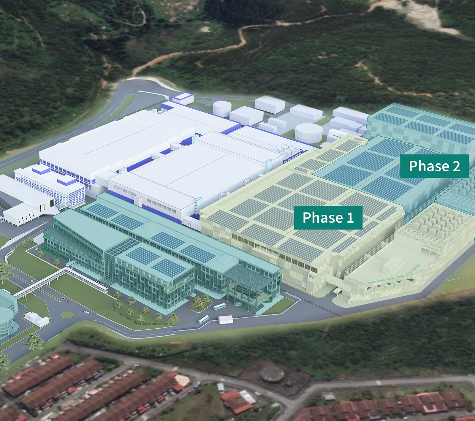
    Infineon to invest EUR 5 billion to expand fab in Malaysia
    Bildquelle nicht angegeben
    Semiconductor-packaging

    Infineon to invest EUR 5 billion to expand fab in Malaysia

    Infineon Technologies will invest EUR 5 billion over the next five years to expand its fab in Kulim, Malaysia into what it calls "the world’s largest
    Veröffentlicht
    04. August 2023
    Lesezeit
    1 Minute
    Rubrik
    Semiconductor-packaging

    The company says the planned expansion is backed by customer commitments covering about five billion euros of new design-wins in automotive and industrial applications as well as about one billion euros in pre-payments.

    “The market for silicon carbide shows accelerating growth, not only in automotive but also in a broad range of industrial applications such as solar, energy storage and high-power EV charging. With the Kulim expansion, we will secure our leadership position in this market,” said Jochen Hanebeck, CEO of Infineon. “With the industry’s leading scale and a unique cost position, we are leveraging our competitive position of best-in-class SiC trench technology, the broadest package portfolio and unrivaled application understanding. These factors are the areas of differentiation and success in the industry.”

    The company says the investment will lead to an annual SiC revenue potential of about seven billion euros by the end of the decade, together with the planned 200-millimeter SiC conversion of Villach and Kulim. This highly competitive manufacturing base will support its SiC market share target of 30% towards the end of the decade.

    “Infineon’s expansion of their world-class silicon carbide facility in Kulim marks a significant milestone in Malaysia’s pursuit of developing advanced manufacturing capabilities, creating high-skilled employment opportunities and positioning the country at the forefront of enabling green technologies, which are crucial to achieving our global sustainable development goals,” said Malaysian Minister of Investment, Trade and Industry (MITI), Tengku Datuk Seri Utama Zafrul Aziz.


    Mehr aus Semiconductor-packaging

    Weitere aktuelle Artikel aus der Rubrik Semiconductor-packaging.

    Alle Semiconductor-packaging-Artikel
    Nanoscribe Expands Photoresin Portfolio for Micro-Optics Fabrication via Two-Photon PolymerizationFoto: Brecht Corbeel / Unsplash
    Semiconductor-packaging

    Nanoscribe Expands Photoresin Portfolio for Micro-Optics Fabrication via Two-Photon Polymerization

    11. November 2026

    Nanoscribe has detailed its range of photoresins engineered for Two-Photon Polymerization (2PP) and Two-Photon Grayscale Lithography (2GL), targeting high-precision micro-optics manufacturing on silicon, glass, and…

    Canon Launches FPA-6400ES6a KrF Lithography System with 400 Wafers-per-Hour ThroughputFoto: Canon Europe (semicon)
    Semiconductor-packaging

    Canon Launches FPA-6400ES6a KrF Lithography System with 400 Wafers-per-Hour Throughput

    10. November 2026

    Canon has announced the FPA-6400ES6a KrF scanner for semiconductor lithography, combining a throughput of 400 wafers per hour with industry-leading overlay accuracy of 4.0 nm and the ability to handle wafer warpage of…

    Fabmatics absorbs SCI business activities under unified brandFoto: Ludovico Ceroseis / Unsplash
    Semiconductor-packaging

    Fabmatics absorbs SCI business activities under unified brand

    6. November 2026

    Fabmatics has integrated the business activities of SCI under the Fabmatics brand, consolidating the acquired expertise within its semiconductor automation portfolio.

    Entegris and Kioxia Expand Partnership on Materials Innovation for Next-Gen 3D Flash MemoryFoto: Louis Reed / Unsplash
    Semiconductor-packaging

    Entegris and Kioxia Expand Partnership on Materials Innovation for Next-Gen 3D Flash Memory

    6. November 2026

    Entegris and Kioxia are deepening their strategic partnership to co-develop materials and process technologies for future BiCS FLASH 3D NAND architectures, using AI, digital-twin modelling and experimental validation at…

    ← Zurück zu Semiconductor-packagingZur Startseite

