Zum Inhalt springen
EPP Europe
  • News
  • Products
  • Applications
  • Technology
  • Semiconductor
  • Inspection
  • Company News
  • Events
EPP Europe
  • Technology
  • Inspection (AOI/AXI)
  • Semiconductor Packaging
  • Company News
  • Products
  • Trade Shows & Events
    EPP Europe Newsletter
    The most important electronics-manufacturing news delivered to your inbox.

    Info

    • Impressum
    • Datenschutz
    • Barrierefreiheit
    • Datenschutzeinstellungen

    Kontakt zur Redaktion

    EPP EuropeKonradin Mediengruppe
    Ernst-Mey-Str. 8, 70771 Leinfelden-Echterdingen

    E-Mail: redaktion@konradin.de
    Folgen Sie uns
    EPP Europe
    © 2026 EPP Europe
    Startseite/Product-news/Artikel
    Imec launches first design pathfinding PDK for N2 node
    Bildquelle nicht angegeben
    Product-news

    Imec launches first design pathfinding PDK for N2 node

    Imec, a research and innovation centre for nanoelectronics and digital technologies, has launched its open process design kit (PDK) with a concomitant
    Veröffentlicht
    19. Februar 2024
    Lesezeit
    3 Minuten
    Rubrik
    Product-news

    Foundry PDKs give chip designers access to a library of tested and proven components to deliver functional and reliable designs. These are usually available to the ecosystem once the technology reaches a critical level of manufacturability. However, restricted access and the need for NDAs have created a high threshold for academia and industry to access advanced technology nodes during their development. Access to imec N2 PDK will help both academia and commercial companies: “If we want to engage a new generation of chip designers, we must provide them early access to the infrastructure needed to develop their design skills on the most advanced technology nodes. The accompanying training courses will get these designers up to speed as quickly as possible and acquaint them with the most recent technology disruptions such as nanosheet devices and wafer backside technology. The design pathfinding PDK will also help companies to transition their designs to future technology nodes and pre-empt scaling bottlenecks for their products.” says Julien Ryckaert, VP Logic Technologies.

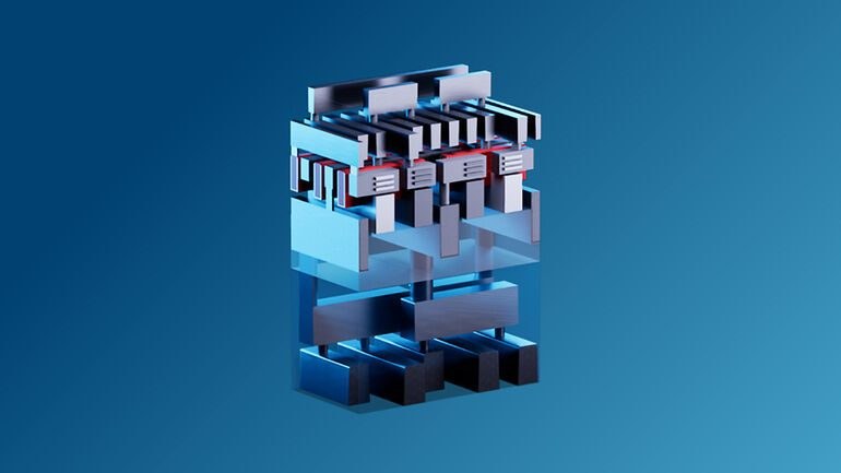
    The design pathfinding PDK contains the necessary infrastructure for digital design based on a set of digital standard cell libraries and SRAM IP macros. In the future, the design pathfinding PDK platform will extend to more advanced nodes (e.g. A14). The training program will start early Q2, teaching subscribers the specificities of the N2 technology node and offering hands-on training on digital design platforms using the Cadence and the Synopsys EDA software.

    “Nurturing an engineering workforce that is equipped with the necessary technology to develop transformational products is critical to the semiconductor industry,” said Brandon Wang, vice president, technical strategy & strategic partnerships at Synopsys. “Imec’s design pathfinding PDK is an excellent example of how industry partnerships can broaden access to advanced process technology for the current and next generation of designers to accelerate their semiconductor innovation. Our collaboration with imec to deliver a certified, AI-driven EDA digital design flow for its N2 PDK enables design teams to prototype and accelerate the transition to next-generation technologies using a virtual PDK-based design environment.”

    “Cadence is committed to working with universities and research institutions to drive innovation and support workforce development for the nano- and microelectronics industry,” said Yoon Kim, VP Cadence Academic Network. “Cadence and imec have a long history of successful collaboration on multiple projects, and the new imec design pathfinding PDK represents a major new milestone for training the next generation of silicon designers. Imec used all the tools in Cadence’s industry leading AI-driven digital and custom / analog full flows to create and validate the design pathfinding PDK, ensuring academia and industry partners have access to a complete Cadence flow at the most advanced nodes, enabling them to transition to the next generation of designs seamlessly.”

    Ar
    Mehr aus Product-news

    Weitere aktuelle Artikel aus der Rubrik Product-news.

    Alle Product-news-Artikel
    Microtronic Introduces Automated Dip & Look Tester for Solderability TestingFoto: gomi / Unsplash
    Product-news

    Microtronic Introduces Automated Dip & Look Tester for Solderability Testing

    12. November 2026

    Microtronic GmbH has launched the D&L Automator, an automated, PC-controlled system for Dip and Look solderability testing, addressing evolving IPC requirements for demonstrating active wetting.

    Indium Corporation's Halogen-Free Solder Paste Indium12.9HF Wins Mexico Technology AwardFoto: Indium Corporation
    Product-news

    Indium Corporation's Halogen-Free Solder Paste Indium12.9HF Wins Mexico Technology Award

    19. Oktober 2026

    Indium Corporation's Indium12.9HF no-clean, halogen-free solder paste has received a Mexico Technology Award in the solder paste category, recognised for its performance in fine-aperture printing and high-density…

    ITW EAE launches ProcessGuard monitoring option for Vitronics Soltec thermal systemsFoto: Nicolas Thomas / Unsplash
    Product-news

    ITW EAE launches ProcessGuard monitoring option for Vitronics Soltec thermal systems

    9. Oktober 2026

    ITW EAE has introduced the ProcessGuard option for its Vitronics Soltec thermal processing equipment, adding real-time monitoring and analytics capabilities to improve process reliability and quality in SMT assembly…

    ITW EAE Launches EcoWave Option for Electrovert Wave Soldering SystemsFoto: ThisisEngineering / Unsplash
    Product-news

    ITW EAE Launches EcoWave Option for Electrovert Wave Soldering Systems

    1. Oktober 2026

    ITW EAE has introduced the EcoWave, a patented next-generation option for its Electrovert wave soldering equipment line, designed to improve process efficiency and reduce environmental impact.

    ← Zurück zu Product-newsZur Startseite