
Zum Inhalt springen
EPP Europe
  • News
  • Products
  • Applications
  • Technology
  • Semiconductor
  • Inspection
  • Company News
  • Events
EPP Europe
  • Technology
  • Inspection (AOI/AXI)
  • Semiconductor Packaging
  • Company News
  • Products
  • Trade Shows & Events
    EPP Europe Newsletter
    The most important electronics-manufacturing news delivered to your inbox.

    Info

    • Impressum
    • Datenschutz
    • Barrierefreiheit
    • Datenschutzeinstellungen

    Kontakt zur Redaktion

    EPP EuropeKonradin Mediengruppe
    Ernst-Mey-Str. 8, 70771 Leinfelden-Echterdingen

    E-Mail: redaktion@konradin.de
    Folgen Sie uns
    EPP Europe
    © 2026 EPP Europe
    Startseite/Semiconductor-packaging/Artikel
    Imec and Buhler Leybold enable high-throughput manufacturing
    Bildquelle nicht angegeben
    Semiconductor-packaging

    Imec and Buhler Leybold enable high-throughput manufacturing

    Buhler Leybold Optics, a supplier of cutting-edge thin-film vacuum coaters and imec, a world-leading research and innovation center in nanoelectronics,
    Veröffentlicht
    13. April 2022
    Lesezeit
    3 Minuten
    Rubrik
    Semiconductor-packaging

    The production of high-resolution low-cost filter-on-chip CMOS detectors for hyperspectral imaging sensors (HSI) for the visible (VIS) and the short-wave infrared (SWIR) range places high demands on thin-film deposition tools. A superior optical performance and low defect levels of the interference filters, combined with maximized wafer throughputs is needed. However, state-of-the-art deposition tools in semiconductor foundries lack a sufficient coating uniformity and optical performance as well as an in-situ thickness control. In the absence of such in-situ layer thickness control, the optical properties of filter stacks with up to hundreds of layers would need to be measured after the deposition of each individual layer. This dramatically reduces wafer throughput, making layer thickness corrections almost impossible.

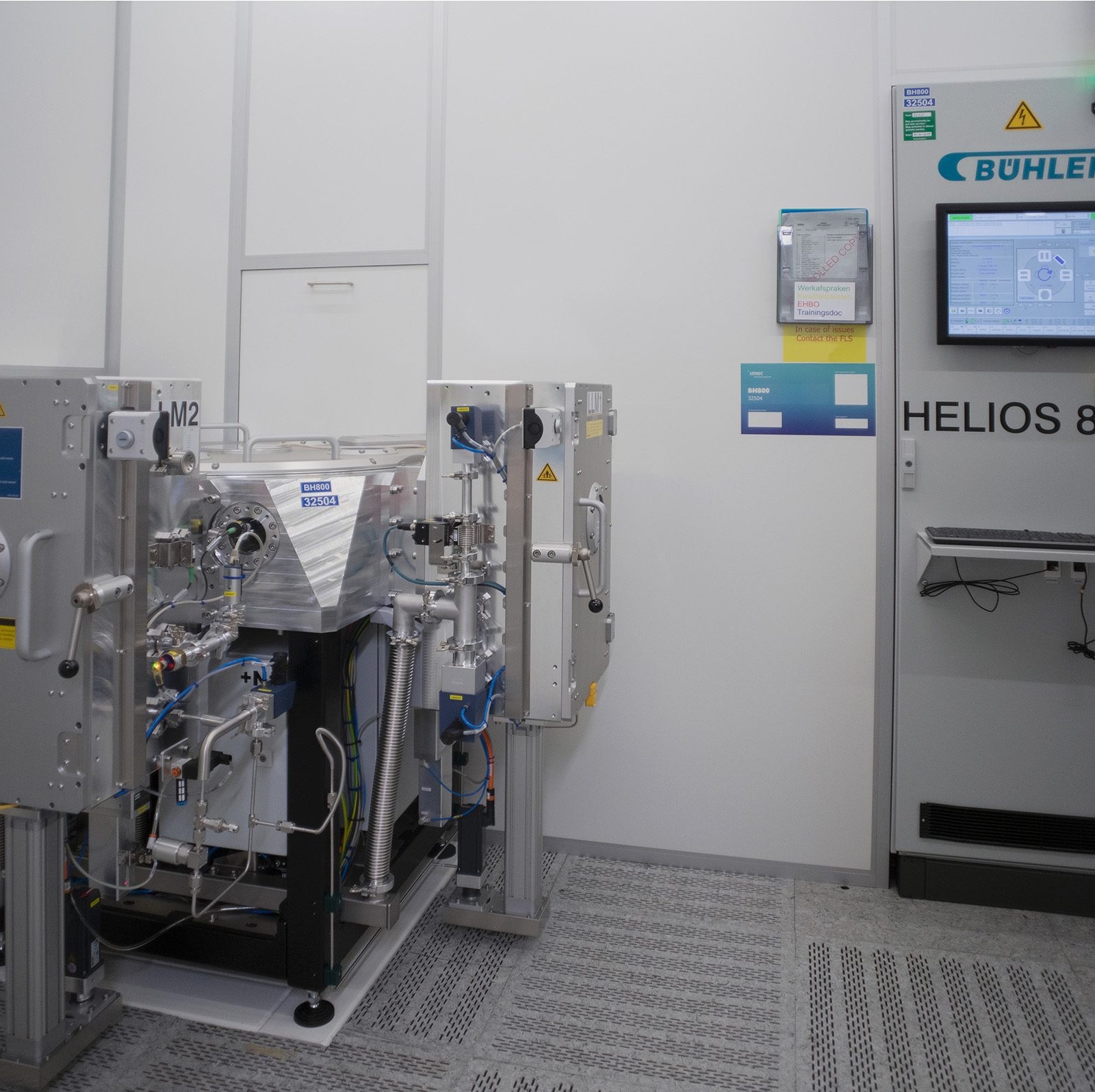
    An in-situ optical monitoring system in the HELIOS 800 Gen II sputter coater allows complex filter coatings with excellent precision in a single production step, in which batches of multiple wafers are processed. Combined with the outstanding single layer quality in terms of thickness uniformity and optical properties as well as its low defect levels, the HELIOS 800 Gen II can pave the way to the next generation of highly resolved HSI sensors.

    Imec and Buhler Leybold Optics engaged in a joint development project, installing a HELIOS 800 Gen II in imec’s 200mm clean room. Within the framework of their collaboration, the HELIOS 800 Gen II was successfully upgraded to meet the extremely high standards of semiconductor manufacturing, with respect to contamination and particles levels. As a result, filters are now within the capabilities to be manufactured at high volume. Currently, imec and Buhler are collaborating to further upgrade the HELIOS 800 Gen II to enable numerous other applications and to enable processing of more complex optical filter architectures, such as photonics devices. This know-how will also be transferred to Buhler’s new sputter coater HELIOS 1200, capable to process 300mm wafers. The joint development project has been extended over the coming years, to enable the next generation of sensors and chips.

    Andy Lambrechts, program director imaging technologies at imec: “Collaborating with Buhler has been of great value to imec. It enabled us to increase the quality of our hyperspectral detectors by decreasing the tolerances on the filters and facilitating more complex filter architectures. The system is available to partners for R&D projects with the support of imec in testing and qualification.”

    Stephan Mingels, team leader M2M development at Buhler:: “Imec enabled Buhler to gain additional experience in front-end semiconductor processing environments. Moreover, the access to imec’s facility including high-end metrology equipment, has been crucial to optimize the performance of the HELIOS 800 Gen II.”


    Mehr aus Semiconductor-packaging

    Weitere aktuelle Artikel aus der Rubrik Semiconductor-packaging.

    Alle Semiconductor-packaging-Artikel
    Nanoscribe Expands Photoresin Portfolio for Micro-Optics Fabrication via Two-Photon PolymerizationFoto: Brecht Corbeel / Unsplash
    Semiconductor-packaging

    Nanoscribe Expands Photoresin Portfolio for Micro-Optics Fabrication via Two-Photon Polymerization

    11. November 2026

    Nanoscribe has detailed its range of photoresins engineered for Two-Photon Polymerization (2PP) and Two-Photon Grayscale Lithography (2GL), targeting high-precision micro-optics manufacturing on silicon, glass, and…

    Canon Launches FPA-6400ES6a KrF Lithography System with 400 Wafers-per-Hour ThroughputFoto: Canon Europe (semicon)
    Semiconductor-packaging

    Canon Launches FPA-6400ES6a KrF Lithography System with 400 Wafers-per-Hour Throughput

    10. November 2026

    Canon has announced the FPA-6400ES6a KrF scanner for semiconductor lithography, combining a throughput of 400 wafers per hour with industry-leading overlay accuracy of 4.0 nm and the ability to handle wafer warpage of…

    Fabmatics absorbs SCI business activities under unified brandFoto: Ludovico Ceroseis / Unsplash
    Semiconductor-packaging

    Fabmatics absorbs SCI business activities under unified brand

    6. November 2026

    Fabmatics has integrated the business activities of SCI under the Fabmatics brand, consolidating the acquired expertise within its semiconductor automation portfolio.

    Entegris and Kioxia Expand Partnership on Materials Innovation for Next-Gen 3D Flash MemoryFoto: Louis Reed / Unsplash
    Semiconductor-packaging

    Entegris and Kioxia Expand Partnership on Materials Innovation for Next-Gen 3D Flash Memory

    6. November 2026

    Entegris and Kioxia are deepening their strategic partnership to co-develop materials and process technologies for future BiCS FLASH 3D NAND architectures, using AI, digital-twin modelling and experimental validation at…

    ← Zurück zu Semiconductor-packagingZur Startseite

