
Zum Inhalt springen
EPP Europe
  • News
  • Products
  • Applications
  • Technology
  • Semiconductor
  • Inspection
  • Company News
  • Events
EPP Europe
  • Technology
  • Inspection (AOI/AXI)
  • Semiconductor Packaging
  • Company News
  • Products
  • Trade Shows & Events
    EPP Europe Newsletter
    The most important electronics-manufacturing news delivered to your inbox.

    Info

    • Impressum
    • Datenschutz
    • Barrierefreiheit
    • Datenschutzeinstellungen

    Kontakt zur Redaktion

    EPP EuropeKonradin Mediengruppe
    Ernst-Mey-Str. 8, 70771 Leinfelden-Echterdingen

    E-Mail: redaktion@konradin.de
    Folgen Sie uns
    EPP Europe
    © 2026 EPP Europe
    Startseite/Semiconductor-packaging/Artikel
    High performance printing processes for Flip Chip bumps
    Bildquelle nicht angegeben
    Semiconductor-packaging

    High performance printing processes for Flip Chip bumps

    To be able to migrate from precision placement of SMD to Semiconductor packaging a knowledge transfer in several areas of the supply chain is going to
    Veröffentlicht
    05. Mai 2022
    Lesezeit
    3 Minuten
    Rubrik
    Semiconductor-packaging

    With this newsletter we like to support SMD and Semiconductor manufacturing with information about very efficient, high performance print processes for Semiconductor Packaging. In the coming months we will share experience specifically about the following topics:

    Semiconductor Backend Processes

    • Bumping
    • Balling
    • Flux printing
    • Chip assembly
    • Chip stack assembly
    • Pre-bowed Chip assembly
    • Copper Pillar chip assembly
    • Chip moulding and filling
    • Conventional LED assembly
    • Min-LED assembly

    Wafer Bumping Process

    This bump technology has some advantages over wire bonding. It can make much shorter electrical connection then wire and achieve better electrical performance. It also can make array with much more I/O accounts means it can process much more data than wire. The wafer bumping process is made for whole wafers to be metalized at one-time, so-called batch process, means this process is much faster than wire bonding. It can end up with lower cost for wafer level CSP (Chip Scale Package) with lower process cost.

    There are two major bumping types. One is solder bump and the other one is cupper pillar bump. Usually solder bump (Wafer Bumping) is used for coarse pitch more than 150µm and cupper pillar fine pitch for less than 150µm. This numbers are based on experience and does not mean to be an absolute rule. Wafer Bumping is a common process to generate “Flip Chip” Bumps on the Wafer Backsite (Components) or on a substrate ( SIP,Chiplets,WLFO , Modules).

    This bumps are needed to make the interconnection between the single component or the package to the PCB or even between the Die stacks in the package.
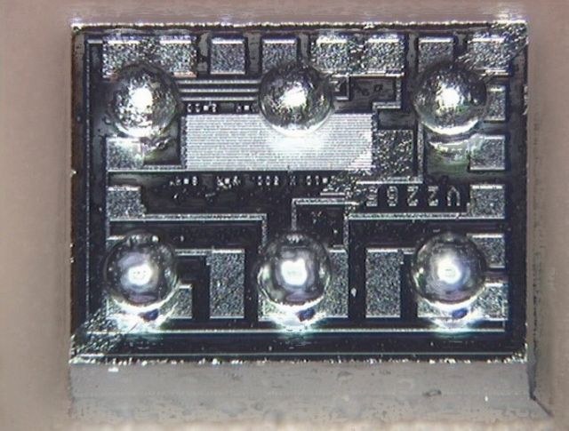
    The wet solder paste gets placed on the Wafer or substrate followed by a reflow process. During the reflow process, the paste will reach the liquidus phase and the surface tension of the solder metal will form a circle segment. (called “BUMP” )

    In order to avoid issues due to unreliable co-planarity in the assembly process, the consistent height of each bump is one of the key performance indicators of this process.
    The height of each bump gets determined by the size of the UBM (Under Bump Metallization) and the volume of the paste deposit. The Paste height and volume is very much depending on the paste and the precision printing tools.

    At Christian Koenen we have developed a specific process on special dedicated Laser Machines to ensure a very small tolerance in terms of Aperture size and shape. Together with dedicated and selected Materials for all our bumping stencils we can ensure a very small tolerance band in terms of bump height. This is very important for either 100 bumps on a substrate or even >600.000 bumps on a Wafer.


    Balling Shemata
    Balling Shemata

    Mehr aus Semiconductor-packaging

    Weitere aktuelle Artikel aus der Rubrik Semiconductor-packaging.

    Alle Semiconductor-packaging-Artikel
    Nanoscribe Expands Photoresin Portfolio for Micro-Optics Fabrication via Two-Photon PolymerizationFoto: Brecht Corbeel / Unsplash
    Semiconductor-packaging

    Nanoscribe Expands Photoresin Portfolio for Micro-Optics Fabrication via Two-Photon Polymerization

    11. November 2026

    Nanoscribe has detailed its range of photoresins engineered for Two-Photon Polymerization (2PP) and Two-Photon Grayscale Lithography (2GL), targeting high-precision micro-optics manufacturing on silicon, glass, and…

    Canon Launches FPA-6400ES6a KrF Lithography System with 400 Wafers-per-Hour ThroughputFoto: Canon Europe (semicon)
    Semiconductor-packaging

    Canon Launches FPA-6400ES6a KrF Lithography System with 400 Wafers-per-Hour Throughput

    10. November 2026

    Canon has announced the FPA-6400ES6a KrF scanner for semiconductor lithography, combining a throughput of 400 wafers per hour with industry-leading overlay accuracy of 4.0 nm and the ability to handle wafer warpage of…

    Fabmatics absorbs SCI business activities under unified brandFoto: Ludovico Ceroseis / Unsplash
    Semiconductor-packaging

    Fabmatics absorbs SCI business activities under unified brand

    6. November 2026

    Fabmatics has integrated the business activities of SCI under the Fabmatics brand, consolidating the acquired expertise within its semiconductor automation portfolio.

    Entegris and Kioxia Expand Partnership on Materials Innovation for Next-Gen 3D Flash MemoryFoto: Louis Reed / Unsplash
    Semiconductor-packaging

    Entegris and Kioxia Expand Partnership on Materials Innovation for Next-Gen 3D Flash Memory

    6. November 2026

    Entegris and Kioxia are deepening their strategic partnership to co-develop materials and process technologies for future BiCS FLASH 3D NAND architectures, using AI, digital-twin modelling and experimental validation at…

    ← Zurück zu Semiconductor-packagingZur Startseite


