
Zum Inhalt springen
EPP Europe
  • News
  • Products
  • Applications
  • Technology
  • Semiconductor
  • Inspection
  • Company News
  • Events
EPP Europe
  • Technology
  • Inspection (AOI/AXI)
  • Semiconductor Packaging
  • Company News
  • Products
  • Trade Shows & Events
    EPP Europe Newsletter
    The most important electronics-manufacturing news delivered to your inbox.

    Info

    • Impressum
    • Datenschutz
    • Barrierefreiheit
    • Datenschutzeinstellungen

    Kontakt zur Redaktion

    EPP EuropeKonradin Mediengruppe
    Ernst-Mey-Str. 8, 70771 Leinfelden-Echterdingen

    E-Mail: redaktion@konradin.de
    Folgen Sie uns
    EPP Europe
    © 2026 EPP Europe
    Startseite/Semiconductor-packaging/Artikel
    High performance printing processes for Chip stack assembly
    Bildquelle nicht angegeben
    Semiconductor-packaging

    High performance printing processes for Chip stack assembly

    To be able to migrate from precision placement of SMD to Semiconductor packaging a knowledge transfer in several areas of the supply chain is going to
    Veröffentlicht
    06. September 2022
    Lesezeit
    3 Minuten
    Rubrik
    Semiconductor-packaging

    With this newsletter we like to support SMD and Semiconductor manufacturing with information about very efficient, high performance print processes for Semiconductor Packaging. In the coming months we will share experience specifically about the following topics:

    Semiconductor Backend Processes

    1. Bumping
    2. Balling
    3. Flux printing
    4. Chip assembly
    5. Chip stack assembly
    6. Pre-bowed Chip assembly
    7. Copper Pillar chip assembly
    8. Chip moulding and filling
    9. Conventional LED assembly
    10. Min-LED assembly

    Chip stack assembly Process

    The difference between wafers and chips lies in the relationship between both components. While the wafer serves as a base for the chip, the chip is implanted in the wafer. Together, they make up the integral part of Semiconductor components that’s commonly used in the field of electronics.
    Microchips are made by building up layers of interconnected patterns on a silicon wafer. The microchip manufacturing process involves hundreds of steps and can take up to four months from design to mass production. The process of putting a semiconductor device or integrated circuit in a package of one form or another usually consists of a series of packaging steps that include: die preparation, die attach, wirebonding, encapsulation or sealing, deflash, lead trimming/forming, and lead finish.

    Microchips are often flat bonded onto a Leadframe or substrate and then another Chip needs to get mounted on top of this Chip. The flat bonding process is done by adhesive, solder paste or sinter materials. Often the Materials need a curing/reflow/sinter process. The first interconnection between the first chip and the Leadframe/substrate will be heated up more times.
    This is not helpful for the connection, because of cracking, intermetallic phases and so on.

    By using a High precision printing process you can print directly on the placed microchip. The material deposition for the next layer can be structured and done without any heating process in between.
    Structuring of the stencils and print process can even perfom for several layers of Microchips.

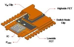
    For an MOSFED , as an example, can this reduce the number of processes and even gives the capability to manufacture the complete Leadframe-die stack in a production line.

    Process steps:

    1. Print under first Chip (even possible in a stepped down leadframe)
    2. Place first chips layer (high side, low side and controller)
    3. Print on top of bottom chips
    4. Place the copper clip on top
    5. One single reflow process at the end

    In attached pictures you can see a schematic and the print on top of the first chip layer before placing the copper clip.

    Beside the possibility to print wet on wet paste, customers also get the opportunity to streamline and improve the process flow to more economic manufacturing costs by improved quality yields.

    Our Semicon teams at Christian Koenen GmbH have extensive process knowledge to design and manufacture customized Semicon stencils. We are offering service support to perform and test printing processes in our Application Lab. Together with our customers we often perform extensive analysis and checks to prove and prepare printing processes for mass production.

    State of the art process equipment and measurement methodology is available to establish and optimize all kind of Wafer printing processes. Please contact our team as soon as you like to learn more about stencil printing for Semicon manufacturing processes.

    Scematic of a MOSFED (source TI)
    Scematic of a MOSFED (source TI)
    Print on chips and leadframe ( wet first print underneath dhe dice)
    Print on chips and leadframe (wet first print underneath dhe dice)
    Print on chip with already 2 dice and 1 clip placed. All wet paste. Before last clip get´s placed.
    Print on chip with already 2 dice and 1 clip placed. All wet paste. Before last clip get´s placed.

    Mehr aus Semiconductor-packaging

    Weitere aktuelle Artikel aus der Rubrik Semiconductor-packaging.

    Alle Semiconductor-packaging-Artikel
    Nanoscribe Expands Photoresin Portfolio for Micro-Optics Fabrication via Two-Photon PolymerizationFoto: Brecht Corbeel / Unsplash
    Semiconductor-packaging

    Nanoscribe Expands Photoresin Portfolio for Micro-Optics Fabrication via Two-Photon Polymerization

    11. November 2026

    Nanoscribe has detailed its range of photoresins engineered for Two-Photon Polymerization (2PP) and Two-Photon Grayscale Lithography (2GL), targeting high-precision micro-optics manufacturing on silicon, glass, and…

    Canon Launches FPA-6400ES6a KrF Lithography System with 400 Wafers-per-Hour ThroughputFoto: Canon Europe (semicon)
    Semiconductor-packaging

    Canon Launches FPA-6400ES6a KrF Lithography System with 400 Wafers-per-Hour Throughput

    10. November 2026

    Canon has announced the FPA-6400ES6a KrF scanner for semiconductor lithography, combining a throughput of 400 wafers per hour with industry-leading overlay accuracy of 4.0 nm and the ability to handle wafer warpage of…

    Fabmatics absorbs SCI business activities under unified brandFoto: Ludovico Ceroseis / Unsplash
    Semiconductor-packaging

    Fabmatics absorbs SCI business activities under unified brand

    6. November 2026

    Fabmatics has integrated the business activities of SCI under the Fabmatics brand, consolidating the acquired expertise within its semiconductor automation portfolio.

    Entegris and Kioxia Expand Partnership on Materials Innovation for Next-Gen 3D Flash MemoryFoto: Louis Reed / Unsplash
    Semiconductor-packaging

    Entegris and Kioxia Expand Partnership on Materials Innovation for Next-Gen 3D Flash Memory

    6. November 2026

    Entegris and Kioxia are deepening their strategic partnership to co-develop materials and process technologies for future BiCS FLASH 3D NAND architectures, using AI, digital-twin modelling and experimental validation at…

    ← Zurück zu Semiconductor-packagingZur Startseite



