
Zum Inhalt springen
EPP Europe
  • News
  • Products
  • Applications
  • Technology
  • Semiconductor
  • Inspection
  • Company News
  • Events
EPP Europe
  • Technology
  • Inspection (AOI/AXI)
  • Semiconductor Packaging
  • Company News
  • Products
  • Trade Shows & Events
    EPP Europe Newsletter
    The most important electronics-manufacturing news delivered to your inbox.

    Info

    • Impressum
    • Datenschutz
    • Barrierefreiheit
    • Datenschutzeinstellungen

    Kontakt zur Redaktion

    EPP EuropeKonradin Mediengruppe
    Ernst-Mey-Str. 8, 70771 Leinfelden-Echterdingen

    E-Mail: redaktion@konradin.de
    Folgen Sie uns
    EPP Europe
    © 2026 EPP Europe
    Startseite/Semiconductor-packaging/Artikel
    High-end performance packaging industry: who are the winners and losers?
    Bildquelle nicht angegeben
    Semiconductor-packaging

    High-end performance packaging industry: who are the winners and losers?

    The market research and strategy consulting company, Yole Développement (Yole), has a comprehensive understanding of the semiconductor packaging industry.
    Veröffentlicht
    22. März 2022
    Lesezeit
    2 Minuten
    Rubrik
    Semiconductor-packaging

    Today, Yole’s semiconductor packaging team releases its annual high-end performance packaging report, High-End Performance Packaging 2022 – Focus on 2.5D/3D Integration. This new study analyzes in detail the challenges and opportunities of this industry. It provides market data on key high-end performance packaging technologies and delivers a valuable understanding of the value chain, infrastructure, and competitive landscape.

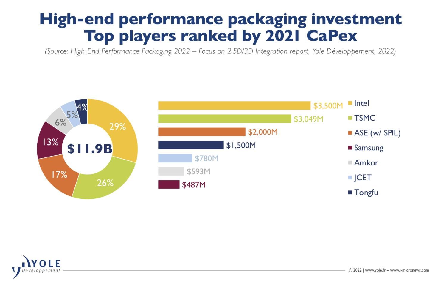
    Stefan Chitoraga, Technology and Market Analyst specializing in Packaging and Assembly at Yole, asserts: “In 2021, CapEx investments of about US$11.6 billion were made in package activity by the top players. Indeed, they are conscious about the enormous importance of fighting the slowdown of Moore’s Law and are adapting their strategies in that direction.”

    Intel is the top investor, with US$3.5 billion. Its 3D chip stacking technology is Foveros, which consists of stacking a die on an active silicon interposer. An embedded multi-die interconnect bridge is its 2.5D packaging solution, utilizing a 55-micron bump pitch. The combination of Foveros and EMIB5 gives birth to Co-EMIB6, used for the Ponte Vecchio GPU7. Intel plans to adopt hybrid bonding technology for Foveros Direct.

    The other leader, TSMC, is following through with US$3.05 billion of CapEx. While securing more business for UHD FO with its InFO8 solutions, TSMC is also defining new system-level roadmaps and technology for 3D SoC9. Its CoWoS platform offers solutions such as RDL10 or silicon interposers, while its LSI platform is a direct competitor for EMIB. TSMC has emerged as a high-end packaging powerhouse with leading FE11 advanced nodes allowing it to dominate next-generation system-level packaging.

    Also on the podium, and boasting a US$2 billion estimated CapEx, ASE is the biggest and only OSAT12 trying to compete with the foundries and IDMs13 in packaging activity. With its FoCoS14 product, ASE is also the only OSAT with a UHD fan-out solution at the moment.
    Yole’s analysts also identified Samsung, just behind ASE. Samsung has its I-Cube technology, which is similar to CoWoS-S15. Samsung is one of the 3D-stacked memory solution leaders, providing HBM and 3DS. Its X-Cube will use hybrid bonding interconnects.

    Today, OSATs don’t have the financial and front-end capabilities to keep pace with the big players like Intel, TSMC, and Samsung in the advanced packaging race. Therefore, they are followers.


    Mehr aus Semiconductor-packaging

    Weitere aktuelle Artikel aus der Rubrik Semiconductor-packaging.

    Alle Semiconductor-packaging-Artikel
    Nanoscribe Expands Photoresin Portfolio for Micro-Optics Fabrication via Two-Photon PolymerizationFoto: Brecht Corbeel / Unsplash
    Semiconductor-packaging

    Nanoscribe Expands Photoresin Portfolio for Micro-Optics Fabrication via Two-Photon Polymerization

    11. November 2026

    Nanoscribe has detailed its range of photoresins engineered for Two-Photon Polymerization (2PP) and Two-Photon Grayscale Lithography (2GL), targeting high-precision micro-optics manufacturing on silicon, glass, and…

    Canon Launches FPA-6400ES6a KrF Lithography System with 400 Wafers-per-Hour ThroughputFoto: Canon Europe (semicon)
    Semiconductor-packaging

    Canon Launches FPA-6400ES6a KrF Lithography System with 400 Wafers-per-Hour Throughput

    10. November 2026

    Canon has announced the FPA-6400ES6a KrF scanner for semiconductor lithography, combining a throughput of 400 wafers per hour with industry-leading overlay accuracy of 4.0 nm and the ability to handle wafer warpage of…

    Fabmatics absorbs SCI business activities under unified brandFoto: Ludovico Ceroseis / Unsplash
    Semiconductor-packaging

    Fabmatics absorbs SCI business activities under unified brand

    6. November 2026

    Fabmatics has integrated the business activities of SCI under the Fabmatics brand, consolidating the acquired expertise within its semiconductor automation portfolio.

    Entegris and Kioxia Expand Partnership on Materials Innovation for Next-Gen 3D Flash MemoryFoto: Louis Reed / Unsplash
    Semiconductor-packaging

    Entegris and Kioxia Expand Partnership on Materials Innovation for Next-Gen 3D Flash Memory

    6. November 2026

    Entegris and Kioxia are deepening their strategic partnership to co-develop materials and process technologies for future BiCS FLASH 3D NAND architectures, using AI, digital-twin modelling and experimental validation at…

    ← Zurück zu Semiconductor-packagingZur Startseite

