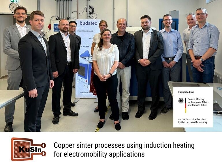
The joint project began in July 2023. Heraeus Electronics met with all partners at the headquarters of the sinter equipment manufacturer Budatec in Berlin for the project launch on July 12–13, 2023. Other partners and participants in this project are: Vitesco Technologies as well as the Chemnitz University of Technology and the Fraunhofer Institutes ENAS and IMWS.
In the KuSIn project, pastes, tools, machines, and processes for inductive sintering of copper particles for (multi-)die and substrate attach (the technical terms for chip and substrate assembly on the circuit carrier) in electromobility, and related power electronics applications will be developed. Silver will be substituted by copper as a joining material in a resource-efficient way. The required higher sinter temperatures and the higher oxidation tendency of copper compared to silver are addressed by fast, selective, and energy-efficient inductive heating. The use of copper as a joining material in combination with induction heating is expected to enable significant improvements in process costs and energy efficiency while maintaining reliability compared to conventional silver sinter processes. Especially the increased use of sintering metal-ceramic substrates on heat sinks or other large-area structures, this could further support the spread of low-temperature sinter technology in power electronics.
Heraeus Electronics will develop copper pastes and processes for inductive sintering of copper particles for die and substrate attach for power electronic assemblies. Both material cost reduction and high-cost process parameters such as sinter temperature, time and pressure will be addressed.
In addition to coordinating the joint project, Vitesco Technologies will apply the new sinter process in the construction of a power module, which will be tested through extensive testing and analysis and compared with the state of the art.
In its subproject, Budatec is designing and implementing a sinter equipment with inductive heating and defined atmospheres. This will enable the inductive copper sinter process to be researched and later industrialized.
Chemnitz University of Technology will design and simulate the core components and the inductive sinter process. In addition, the sub-project includes the realization of an inductive sinter module for integration into the sinter equipment.
The Fraunhofer Institutes ENAS and IMWS will develop the induction coil and the copper sinter process as well as perform material diagnostics and reliability assessments in their subproject. For this purpose, Fraunhofer ENAS will conceptualize miniaturized induction coils for the inductive sinter module, realize them by means of microtechnological processes, and research the application of copper sinter paste in the inductive copper sinter process. The Fraunhofer IMWS is dedicated to microstructure-based research of copper sinter pastes during development and processing as well as to material interactions (joint formation, aging, degradation) in the inductively sintered contact interface based on non-destructive investigation methods, high precision target preparations, highest resolution analysis techniques as well as micromechanical, thermographic, electrical, and chemical characterization methods.