
Zum Inhalt springen
EPP Europe
  • News
  • Products
  • Applications
  • Technology
  • Semiconductor
  • Inspection
  • Company News
  • Events
EPP Europe
  • Technology
  • Inspection (AOI/AXI)
  • Semiconductor Packaging
  • Company News
  • Products
  • Trade Shows & Events
    EPP Europe Newsletter
    The most important electronics-manufacturing news delivered to your inbox.

    Info

    • Impressum
    • Datenschutz
    • Barrierefreiheit
    • Datenschutzeinstellungen

    Kontakt zur Redaktion

    EPP EuropeKonradin Mediengruppe
    Ernst-Mey-Str. 8, 70771 Leinfelden-Echterdingen

    E-Mail: redaktion@konradin.de
    Folgen Sie uns
    EPP Europe
    © 2026 EPP Europe
    Startseite/Semiconductor-packaging/Artikel
    Heraeus Electronics participates in EU project All2GaN for power electronics
    Bildquelle nicht angegeben
    Semiconductor-packaging

    Heraeus Electronics participates in EU project All2GaN for power electronics

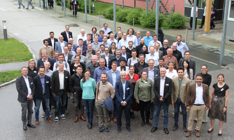
    Heraeus Electronics has announced its participation in the EU-funded research project ALL2GaN (Affordable smart GaN IC solutions for greener
    Veröffentlicht
    06. Juli 2023
    Lesezeit
    2 Minuten
    Rubrik
    Semiconductor-packaging

    Energy efficiency plays a vital role in reducing carbon emissions and achieving climate neutrality. Gallium nitride (GaN) chips have emerged as a game-changing technology in this regard. They deliver more power in a compact size, ensuring highly efficient energy conversion and minimizing the carbon footprint of digital devices.

    As part of the ALL2GaN project, Heraeus Electronics will focus on developing innovative packaging materials specifically tailored for the new generation of GaN chips. These materials will support the miniaturization and high power density of GaN chips, enabling their seamless integration into a wide range of applications.

    The project aims to create a modular and easily adaptable GaN power semiconductor toolbox, allowing for swift integration into various applications. This versatility will result in increased energy efficiency and reduced CO2 emissions. Telecommunications, data centers, server farms, e-mobility, renewable energies and smart grid solutions are among the sectors that will benefit from the highly integrable GaN chip generation „Made in Europe.“ Projections indicate that this new GaN chip generation can reduce energy losses in applications by an average of 30 percent, saving approximately 218 megatons of CO2 worldwide.

    “ALL2GaN is a significant step towards achieving the European Green Deal goals. By developing cost-efficient and easily integrable GaN chips, we are accelerating the transition towards a greener and more sustainable future,” said Dr. Michael Jörger, Head of Business Line Power Electronic Materials. “We are excited to collaborate with leading industry partners and contribute to the advancement of energy-saving technologies that will benefit multiple sectors and reduce the carbon footprint.”

    The ALL2GaN project aligns with the European Union‘s objectives to drive climate neutrality, promote sustainable growth, and establish a competitive and resilient European industry. It is a key building block in the European Chip Act, fostering the development of a robust European chip ecosystem and contributing to European tech sovereignty.

    For more information about the ALL2GaN project, please visit the official project website.

    Mehr aus Semiconductor-packaging

    Weitere aktuelle Artikel aus der Rubrik Semiconductor-packaging.

    Alle Semiconductor-packaging-Artikel
    Nanoscribe Expands Photoresin Portfolio for Micro-Optics Fabrication via Two-Photon PolymerizationFoto: Brecht Corbeel / Unsplash
    Semiconductor-packaging

    Nanoscribe Expands Photoresin Portfolio for Micro-Optics Fabrication via Two-Photon Polymerization

    11. November 2026

    Nanoscribe has detailed its range of photoresins engineered for Two-Photon Polymerization (2PP) and Two-Photon Grayscale Lithography (2GL), targeting high-precision micro-optics manufacturing on silicon, glass, and…

    Canon Launches FPA-6400ES6a KrF Lithography System with 400 Wafers-per-Hour ThroughputFoto: Canon Europe (semicon)
    Semiconductor-packaging

    Canon Launches FPA-6400ES6a KrF Lithography System with 400 Wafers-per-Hour Throughput

    10. November 2026

    Canon has announced the FPA-6400ES6a KrF scanner for semiconductor lithography, combining a throughput of 400 wafers per hour with industry-leading overlay accuracy of 4.0 nm and the ability to handle wafer warpage of…

    Fabmatics absorbs SCI business activities under unified brandFoto: Ludovico Ceroseis / Unsplash
    Semiconductor-packaging

    Fabmatics absorbs SCI business activities under unified brand

    6. November 2026

    Fabmatics has integrated the business activities of SCI under the Fabmatics brand, consolidating the acquired expertise within its semiconductor automation portfolio.

    Entegris and Kioxia Expand Partnership on Materials Innovation for Next-Gen 3D Flash MemoryFoto: Louis Reed / Unsplash
    Semiconductor-packaging

    Entegris and Kioxia Expand Partnership on Materials Innovation for Next-Gen 3D Flash Memory

    6. November 2026

    Entegris and Kioxia are deepening their strategic partnership to co-develop materials and process technologies for future BiCS FLASH 3D NAND architectures, using AI, digital-twin modelling and experimental validation at…

    ← Zurück zu Semiconductor-packagingZur Startseite


