
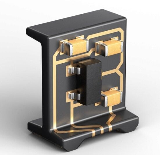
Modern electronic assemblies are becoming more and more complex with an increasing number of components. This makes it difficult to fit all parts into the limited space available for printed circuit boards (PCBs). To meet these challenges, engineers are using miniaturized components and flexible or rigid-flex PCBs. There is, however, a very strong trend is 3D packaging. Many applications require a lot of manual work, which is inefficient and error-prone. A comprehensive analysis of manual work steps in PCB assemblies revealed that a large percentage of these errors are due to the vertical assembly of one or more electronic components to the main PCB. The 3D-Circuits Component Carrier addresses these points.
Vertical placement of electronic components
Vertical placement of electronic components on a PCB is challenging because it usually requires manual assembly. This can be time-consuming, labour-intensive and lead to errors. The Chip Carrier is suitable for a wide range of applications, including Hall effect and acceleration sensors, ICs, and LED applications. It is also compatible with multiple soldering processes, making it a versatile and flexible solution.
Some of the benefits include:
- Eliminates the need for manual assembly
- Improves accuracy and repeatability
- Compatible with multiple soldering processes
- Versatile and variable
The assembled component carrier can be fully automated as a sub-assembly on standard SMT machines, which can simplify the production process and offers the potential to miniaturize your final product.
Eliminating piggyback boards
Piggyback PCBs are two separate PCBs that are stacked on top of each other. They are often used when there is not enough space for a single PCB. 3D-Circuits offer a number of benefits over piggyback PCBs. They are smaller, lighter, and easier to manufacture. They also offer greater design flexibility and can be processed fully automatically with SMT machines. As a result, 3D circuits are becoming increasingly popular in a variety of applications in medical, automotive as well as in industrial and consumer electronics.
The component carrier can be used as an adapter for alternative packaging. This is particularly useful if your original component is no longer available, but you want to use another component with the same function. It adapts the footprint of the alternative package to the footprint of the original component. There is no need to change the layout of the main PCB and this means validation and qualification loops can be avoided, this saves you time and money.