
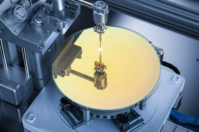
The Graphene Flagship, an initiative to advance Europe’s strategic autonomy in technologies that rely on graphene and other 2D materials, hosted a symposium from 11–12 June to celebrate the successes of its €20 million 2D Experimental Pilot Line (2D-EPL) project. Representing the first graphene foundry to integrate graphene and other 2D materials into semiconductor devices, the symposium demonstrated the 2D-EPL’s progress in creating an ecosystem for 2D materials within electronics, photonics and biomedical devices.
Beginning in October 2020, the four-year project is the culmination of many of the Graphene Flagship’s efforts to bring graphene and related materials (GRM) out of the laboratory and into scalable commercial production and usage. As the 2D-EPL is now in its fourth and final year, the symposium presented significant outcomes from the project and outline future directions.
2D-EPL project
Initially, the 2D-EPL project was constructed around two pillars. The first, focused on prototyping and wafer fabrication, offered academics, researchers and private companies a first-of-its-kind opportunity to test and prototype novel ideas for 2D material devices. Five experimental multi-project wafer (MPW) runs have enabled low cost, large-scale prototype development.
The other pillar has been focused on process enablement, featuring the construction of two bespoke new tools. This includes a metalorganic chemical vapour deposition (MOCVD) reactor from Aixtron and automated 2D layer transfer tool by SUSS MicroTec. Creation of these tools has enabled thorough testing and modification of 2D material growth and layer transfer processes, providing an essential foundation for achieving high production capabilities in the future.
“We’re very pleased with the project results so far and are looking forward to sharing our progress with the wider scientific community,” explained Inge Asselberghs, 2D-EPL division leader at imec and symposium lead. “As we’re now approaching the sixth and last MPW run of the project, it’s our ambition to go in a full sequence from growth to transfer, using the new tooling and applying the lessons we’ve learnt so far to make this run our most successful yet.”
“The Pilot Line is not just about the hard data and scientific and technological advances that we have gathered together, but also — and perhaps even more importantly — the personal interactions that have created a playground for cross-fertilisation of ideas for the future of 2D materials innovation in Europe,” adds Patrik Johansson, director of the Graphene Flagship. “And as the global graphene market is set to grow exponentially in size, from an annual revenue of 380 million US$ in 2022 to 1.5 billion US$ in just five years, projects like the 2D-EPL are vital in keeping Europe at the forefront of development and innovation.“
This commitment to European development is further solidified through the actions of the Graphene Flagship’s former director Jari Kinaret, who is currently taking leadership of the Chips Joint Undertaking. With this initiative, the European Commission aims to reinforce Europe’s position as a technological leader in the semiconductor industry and secure industrial independence, goals that are central to the 2D-EPL project.



