
Zum Inhalt springen
EPP Europe
  • News
  • Products
  • Applications
  • Technology
  • Semiconductor
  • Inspection
  • Company News
  • Events
EPP Europe
  • Technology
  • Inspection (AOI/AXI)
  • Semiconductor Packaging
  • Company News
  • Products
  • Trade Shows & Events
    EPP Europe Newsletter
    The most important electronics-manufacturing news delivered to your inbox.

    Info

    • Impressum
    • Datenschutz
    • Barrierefreiheit
    • Datenschutzeinstellungen

    Kontakt zur Redaktion

    EPP EuropeKonradin Mediengruppe
    Ernst-Mey-Str. 8, 70771 Leinfelden-Echterdingen

    E-Mail: redaktion@konradin.de
    Folgen Sie uns
    EPP Europe
    © 2026 EPP Europe
    Startseite/Semiconductor-packaging/Artikel
    Global fab equipment spending to recover in 2024
    Bildquelle nicht angegeben
    Semiconductor-packaging

    Global fab equipment spending to recover in 2024

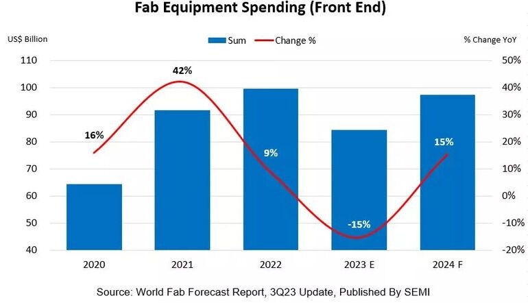
    Global fab equipment spending for front-end facilities in 2023 is expected to decline 15% year-over-year (YoY) to USD 84 billion (EUR 79 billion) from a
    Veröffentlicht
    12. September 2023
    Lesezeit
    3 Minuten
    Rubrik
    Semiconductor-packaging

    Next year’s fab equipment spending recovery will be partly driven by the end of the semiconductor inventory correction in 2023 and strengthening demand for semiconductors in the high-performance computing (HPC) and memory segments.

    “The 2023 decline in equipment investment is proving shallower and the 2024 rebound stronger than expected earlier this year,” said Ajit Manocha, SEMI president and CEO. “The trend suggests the semiconductor industry is turning the corner on the downturn and on a path back to robust growth fueled by healthy chip demand.”

    Covering 2022 to 2024, the report shows the global semiconductor industry increasing capacity by 5% this year after an 8% rise in 2022. Capacity growth is expected to continue in 2024, climbing 6%.

    Foundry segment

    The foundry segment is expected to lead the semiconductor expansion in 2023 with USD 49 billion in investments, 1% growth, and USD 51.5 billion in spending in 2024, a 5% increase as investment continues in leading-edge and mature process nodes. Memory spending is forecast to stage a strong comeback in 2024 with a 65% increase to USD 27 billion after a 46% decline in 2023. Specifically, DRAM investments are expected to decline 19% YoY to USD 11 billion in 2023 but recover to USD15 billion, a 40% annual jump, in 2024. NAND spending is projected to mirror that trend, decreasing 67% to USD 6 billion in 2023 but surging 113% to USD 12.1 billion in 2024. MPU investments are expected to remain flat in 2023 and increase 16% to USD 9 billion in 2024.

    Taiwan leads spending

    Taiwan is expected to retain the global lead in fab equipment spending in 2024 with USD 23 billion in investments, a 4% YoY increase. Korea is projected to rank second in spending, with an estimated USD 22 billion in investments in 2024, a 41% jump from this year reflecting a memory sector recovery. With export controls expected to limit China’s spending in leading-edge technologies and foreign investment, the region is forecast to place third in equipment spending worldwide in 2024 at USD 20 billion, a decline from 2023 levels. Despite the constraints, Chinese foundry suppliers and IDMs are expected to continue investments in mature process nodes.

    The Americas is expected to remain the fourth largest region in spending, reaching a historic high of US$14 billion in investments in 2024, a 23% YoY increase. The Europe and Mideast region is also forecast to log record investments next year, increasing spending by 41.5% to US$8 billion. Fab equipment spending in Japan and Southeast Asia is expected to increase to USD 7 billion and USD 3 billion, respectively, in 2024.


    Mehr aus Semiconductor-packaging

    Weitere aktuelle Artikel aus der Rubrik Semiconductor-packaging.

    Alle Semiconductor-packaging-Artikel
    Nanoscribe Expands Photoresin Portfolio for Micro-Optics Fabrication via Two-Photon PolymerizationFoto: Brecht Corbeel / Unsplash
    Semiconductor-packaging

    Nanoscribe Expands Photoresin Portfolio for Micro-Optics Fabrication via Two-Photon Polymerization

    11. November 2026

    Nanoscribe has detailed its range of photoresins engineered for Two-Photon Polymerization (2PP) and Two-Photon Grayscale Lithography (2GL), targeting high-precision micro-optics manufacturing on silicon, glass, and…

    Canon Launches FPA-6400ES6a KrF Lithography System with 400 Wafers-per-Hour ThroughputFoto: Canon Europe (semicon)
    Semiconductor-packaging

    Canon Launches FPA-6400ES6a KrF Lithography System with 400 Wafers-per-Hour Throughput

    10. November 2026

    Canon has announced the FPA-6400ES6a KrF scanner for semiconductor lithography, combining a throughput of 400 wafers per hour with industry-leading overlay accuracy of 4.0 nm and the ability to handle wafer warpage of…

    Fabmatics absorbs SCI business activities under unified brandFoto: Ludovico Ceroseis / Unsplash
    Semiconductor-packaging

    Fabmatics absorbs SCI business activities under unified brand

    6. November 2026

    Fabmatics has integrated the business activities of SCI under the Fabmatics brand, consolidating the acquired expertise within its semiconductor automation portfolio.

    Entegris and Kioxia Expand Partnership on Materials Innovation for Next-Gen 3D Flash MemoryFoto: Louis Reed / Unsplash
    Semiconductor-packaging

    Entegris and Kioxia Expand Partnership on Materials Innovation for Next-Gen 3D Flash Memory

    6. November 2026

    Entegris and Kioxia are deepening their strategic partnership to co-develop materials and process technologies for future BiCS FLASH 3D NAND architectures, using AI, digital-twin modelling and experimental validation at…

    ← Zurück zu Semiconductor-packagingZur Startseite

