
Zum Inhalt springen
EPP Europe
  • News
  • Products
  • Applications
  • Technology
  • Semiconductor
  • Inspection
  • Company News
  • Events
EPP Europe
  • Technology
  • Inspection (AOI/AXI)
  • Semiconductor Packaging
  • Company News
  • Products
  • Trade Shows & Events
    EPP Europe Newsletter
    The most important electronics-manufacturing news delivered to your inbox.

    Info

    • Impressum
    • Datenschutz
    • Barrierefreiheit
    • Datenschutzeinstellungen

    Kontakt zur Redaktion

    EPP EuropeKonradin Mediengruppe
    Ernst-Mey-Str. 8, 70771 Leinfelden-Echterdingen

    E-Mail: redaktion@konradin.de
    Folgen Sie uns
    EPP Europe
    © 2026 EPP Europe
    Startseite/News/Artikel
    Generation of debonders and warpage adjusters in eWLB processes
    Bildquelle nicht angegeben
    News

    Generation of debonders and warpage adjusters in eWLB processes

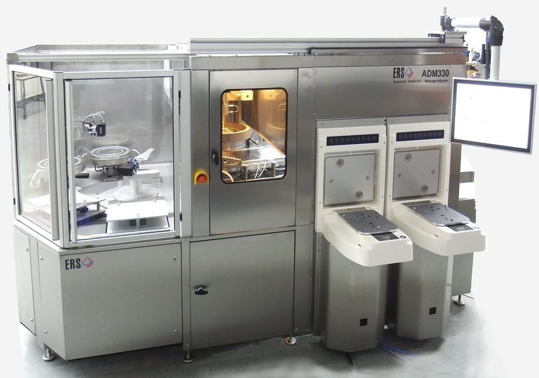
    ERS electronic GmbH introduced systems that are targeting the thermal debonding and warpage adjusting in eWLB processes for 300/330 mm wafer processing.
    Veröffentlicht
    22. Mai 2017
    Lesezeit
    2 Minuten
    Rubrik
    News

    ERS electronic GmbH, a leader in the market of thermal test solutions for semiconductor production, is introducing two new innovative products. The systems are targeting the thermal debonding and warpage adjusting in eWLB (embedded Wafer Level Ball Grid Array) processes for 300/330 mm wafer processing. With their innovative features, these machines enable semiconductor manufacturers to increase both throughput and yield.

    The ERS ADM330 is designed for the thermal debonding of eWLB style wafers without human intervention at high precision and with unmatched repeatability, resulting in high and predictable process quality and thus guaranteeing high yield. The two handling robots accept wafers with a maximum warpage of ± 5 mm; after the adjustment step, the warpage is typically less than 500 µm.

    With built-in OCR/BCR capabilities, the ERS ADM330 allows for automated exchange of batch parameters with process control systems through its optional SECCS/GEM interface. This enables operators to drive integration into higher-level factory IT systems one step further. Its integrated laser-scribing chamber allows for continuous and complete monitoring of production-relevant data.

    The ERS WAT 330 is a fully automated warpage adjust tool for 300/330 mm wafers that can handle up to four FOUPs concurrently. With its specially designed proprietary Warpage Adjust Technology, also included in the ADM330, this system can form a wide variety of eWLB wafers at various processing stages. The resulting wafer shape can be matched to the handling specifications of the downstream tool.

    Its three operation modes give users of the ERS WAT 330 a maximum of flexibility in high-volume production environments. The system can be used as a warpage measurement station, as a warpage adjust station or as a combined tool to measure, adjust and monitor warpage. In warpage adjust mode, the system can reduce wafer warpage from ± 5 mm to below 500 µm.

    Meeting the SEMI E84 interface specifications for factory automation, both systems are future-proof with respect to next-generation digital factory concepts.


    www.brandandimage.de

    Mehr aus News

    Weitere aktuelle Artikel aus der Rubrik News.

    Alle News-Artikel
    Microtronic Takes on Distribution of iRaptor EYE Thermal Profiler in GermanyFoto: Laurens van der Drift / Unsplash
    News

    Microtronic Takes on Distribution of iRaptor EYE Thermal Profiler in Germany

    9. November 2026

    German distributor Microtronic has announced it will represent iRaptor LDA and its EYE thermal profiler in Germany. The Portuguese developer's system extends beyond conventional 2D time-temperature profiling by…

    Indium Corporation Presents Solder Materials Research at SMTAI 2026Foto: Indium Corporation
    News

    Indium Corporation Presents Solder Materials Research at SMTAI 2026

    29. Oktober 2026
    ← Zurück zu NewsZur Startseite

    Indium Corporation is fielding five specialists at SMTA International 2026 to present new findings on solder paste rheology, BGA ball alloy selection for lower-temperature reflow, and the effect of print gap on paste…

    KYZEN to Present AQUANOX Aqueous Cleaning Chemistries at SMTA International 2026Foto: Vishnu Mohanan / Unsplash
    News

    KYZEN to Present AQUANOX Aqueous Cleaning Chemistries at SMTA International 2026

    16. Oktober 2026

    KYZEN will exhibit its AQUANOX line of aqueous electronics cleaning chemistries at SMTA International, October 27–29, 2026, highlighting prolonged bath life as a process efficiency and cost-reduction lever for…

    Fuji America and Cybord Partner to Integrate Visual AI Component Inspection into SMT LinesFoto: Cybord
    News

    Fuji America and Cybord Partner to Integrate Visual AI Component Inspection into SMT Lines

    29. August 2026

    Fuji America Corporation and Cybord have announced a strategic partnership to embed AI-powered component analytics directly into SMT production lines, enabling 100% real-time inspection of electronic components during…

