
Zum Inhalt springen
EPP Europe
  • News
  • Products
  • Applications
  • Technology
  • Semiconductor
  • Inspection
  • Company News
  • Events
EPP Europe
  • Technology
  • Inspection (AOI/AXI)
  • Semiconductor Packaging
  • Company News
  • Products
  • Trade Shows & Events
    EPP Europe Newsletter
    The most important electronics-manufacturing news delivered to your inbox.

    Info

    • Impressum
    • Datenschutz
    • Barrierefreiheit
    • Datenschutzeinstellungen

    Kontakt zur Redaktion

    EPP EuropeKonradin Mediengruppe
    Ernst-Mey-Str. 8, 70771 Leinfelden-Echterdingen

    E-Mail: redaktion@konradin.de
    Folgen Sie uns
    EPP Europe
    © 2026 EPP Europe
    Startseite/Semiconductor-packaging/Artikel
    Fraunhofer IMWS research contributes to GaN device process optimisation
    Bildquelle nicht angegeben
    Semiconductor-packaging

    Fraunhofer IMWS research contributes to GaN device process optimisation

    German research institute, Fraunhofer Institute for Microstructure of Materials and Systems (IMWS) says it has contributed to process and reliability
    Veröffentlicht
    06. März 2023
    Lesezeit
    2 Minuten
    Rubrik
    Semiconductor-packaging

    In the recently completed research project, which ran for 3.5 years from 2019 to 2022, a consortium of 26 European partners from science and industry, under the leadership of Infineon Austria, set themselves the task of harnessing the advantages of GaN technology along the entire value chain, from process development, design, assembly and interconnection technologies to integrated system solutions.

    While GaN-based power semiconductors offer higher performance in a smaller space, and thus save energy and resources, the special chemical-physical material properties and the structure of high-electron mobility transistors raises questions. “The high electric field strengths and enormous current and power densities with correspondingly high material stress in these very compact components pose particular challenges.“, explained Frank Altmann, Head of the Business Unit ‘Materials and Components for Electronics’ at the Fraunhofer IMWS.

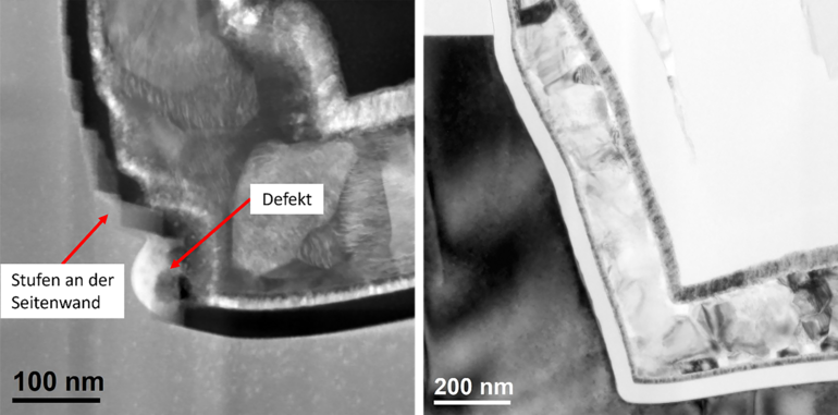
    With high-resolution analysis procedures and innovative fault diagnosis methods the Fraunhofer Institute for Microstructure of Materials and Systems IMWS contributed to process optimisation and increasing the reliability of the GaN devices.

    “We are researching specific critical defects or GaN-specific degradation processes in order to be able to detect, understand and thus avoid new failure modes as early as possible,” said Altmann.

    Leakage current paths, for example, were localised after reliability testing and investigated microstructurally to determine their cause. As such, a new defect signature was identified that led to the premature electrical breakdown of special semi-vertical GaN transistors. On the basis of these findings, the manufacturing process could be systematically optimised.

    With nanoindentation testing in combination with acoustic emission, IMWS scientists were able to detect hidden microcracks under the metallisation layers of bond pads. The above mentioned methodology was applied and evaluated on different processed samples of the project partners and the related defect structures were investigated by electron microscopy analyses.


    /www.imws.fraunhofer.de/en

    Mehr aus Semiconductor-packaging

    Weitere aktuelle Artikel aus der Rubrik Semiconductor-packaging.

    Alle Semiconductor-packaging-Artikel
    Nanoscribe Expands Photoresin Portfolio for Micro-Optics Fabrication via Two-Photon PolymerizationFoto: Brecht Corbeel / Unsplash
    Semiconductor-packaging

    Nanoscribe Expands Photoresin Portfolio for Micro-Optics Fabrication via Two-Photon Polymerization

    11. November 2026

    Nanoscribe has detailed its range of photoresins engineered for Two-Photon Polymerization (2PP) and Two-Photon Grayscale Lithography (2GL), targeting high-precision micro-optics manufacturing on silicon, glass, and…

    Canon Launches FPA-6400ES6a KrF Lithography System with 400 Wafers-per-Hour ThroughputFoto: Canon Europe (semicon)
    Semiconductor-packaging

    Canon Launches FPA-6400ES6a KrF Lithography System with 400 Wafers-per-Hour Throughput

    10. November 2026

    Canon has announced the FPA-6400ES6a KrF scanner for semiconductor lithography, combining a throughput of 400 wafers per hour with industry-leading overlay accuracy of 4.0 nm and the ability to handle wafer warpage of…

    Fabmatics absorbs SCI business activities under unified brandFoto: Ludovico Ceroseis / Unsplash
    Semiconductor-packaging

    Fabmatics absorbs SCI business activities under unified brand

    6. November 2026

    Fabmatics has integrated the business activities of SCI under the Fabmatics brand, consolidating the acquired expertise within its semiconductor automation portfolio.

    Entegris and Kioxia Expand Partnership on Materials Innovation for Next-Gen 3D Flash MemoryFoto: Louis Reed / Unsplash
    Semiconductor-packaging

    Entegris and Kioxia Expand Partnership on Materials Innovation for Next-Gen 3D Flash Memory

    6. November 2026

    Entegris and Kioxia are deepening their strategic partnership to co-develop materials and process technologies for future BiCS FLASH 3D NAND architectures, using AI, digital-twin modelling and experimental validation at…

    ← Zurück zu Semiconductor-packagingZur Startseite

