
Heike Schlessmann, Seho; Olaf Nusche, Technolab
The many ways to detect production-related defects in the board assembly are often too time absorbing, too expensive, or they require the destruction of the product. So far, X-ray has been the most suitable method to examine hidden solder joints as acquainted with BGAs or flip chips, etc. With X-ray, it is possible to detect manufacturing flaws such as solder bridging, voids or wrong orientation. However, this technique is not suited to verify surface-structures, nor to detect flux residues or similar. Therefore, the optimum alternative remains optical solder joint inspection. But special difficulties require specialized inspection instruments. Consequently, different systems must be used which leads to high investment expenses.
Until now, it was not possible to examine each solder joint under every field-array package. With the currently available inspection instruments, only the outside-placed solder joint rows of packages can be achieved. This leads to problems, particularly with flipped advanced devices of all kinds, such BGAs. The center of these components is generally regarded as the critical point. Material outgassing may lead quickly to cold solder joints or bridging. Thus, it is often necessary to inspect the center area directly under the package to draw conclusions for a process free of faults. For example, the internal deformation versus homogeneously formed balls at the perimeter may lead to the assumption of insufficient energy absorption.
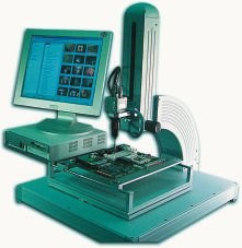
Non-destructive inspection is of course the industry standard method in the optical verification of board assemblies, and it has to offer the capability to inspect even joints difficult to access. Further-more, such equipment has to support easy handling of the assemblies, must meet the ISO 9000 quality assurance guidelines and be able to monitor and quickly interpret the process or quality data, respectively. Seho’s mi-cro inspection equipment A2IS (area-array inspection system) features quick-exchange len-ses, and covers nearly the whole spectrum of board assemblies. This stretches from imaging of complete assemblies through to the macro zoom level – similar to stereo microscopes – and even offers specialized optics for endos-copic applications.
This open-design system can adapt different lenses quickly and easily without any tool. Cutting edge technology such as a camera with digital zoom has been integrated. With its unique concept, the system is able to inspect the bottom side of soldered components (BGAs or PGAs), and it may even check the interior of relay casings. Configured as endoscope for flexible applications, it offers a possibility to control every single solder joint. With an endo-scope diameter of only 0.32mm, even those solder joints that are extremely difficult to access can be seen, as the highly flexible fiber ending can reach virtually every spot.
In addition to the flexible endoscope, a rigid version can be integrated. This rigid version then allows inspecting the outside packaging rows soldered onto assemblies from the side. Typically, the rigid endo-scope is used, for example, to examine a solder joint surface or the soldered I/Osof PLCCs. The ending of the rigid endo-scope has a diameter of only 2mm. Consequently, even very densely packaged assemblies may be inspected without difficulties.
As an aid for orientation or to obtain a quick survey of an assembly, the system features lenses which supply views covering the area of 250 x 250mm down to 0.5mm as full-screen format. The assembly is placed in a fixture which features correction capability in X, Y and theta directions. The optics, which can be easily exchanged, are adapted in the Z direction guide. Comprehensive analysis software complements the inspection system. It operates with an image database which remarkab-ly facilitates the process of working with the inspection results by its networking ability.
The image database supports thorough analysis and provides quick access to data and visual descriptions. By connecting the respective data and images, up-to-date reports may be called up by just simply pushing a button, without using sophisticated procedures. Process parameters, for example arrows, text or gauging functions, are also integrated. To cover a wide range of process variations, single images as well as sequences can be stored. The software is completed with a defect-data file to quickly compare the real-time images with stored defect examples. Thus, the inspection system can also be used by less experienced staff. The defect-data file contains approximately 800 images at delivery, and is ideally suited for staff training using explanations on a visual base.
Moderne Baugruppenfertigung basiert nicht nur auf kontinuierlicher Überwachung der Produktqualität, sondern auch auf fortlaufend optimierten Prozessen. Manuelle Inspektionsgeräte liefern dafür wertvolle Informationen. Sie sind insbesondere hilfreich bei der Applikation von Advanced-Packages wie BGA, CSP oder Flip-Chip, um unter den dort reichlich limitierten Platzbedingungen deren Anschlüsse zu verifizieren.
La fabrication moderne de modules ne se base pas uniquement sur la surveillance continue de la qualité des produits mais également sur l’optimisation permanente des processus. Les appareils d’inspection manuelle fournissent à cet égard de précieuses informations. Ils sont particulièrement utiles dans l’application des Advanced-Packages comme les BGA, les CSP ou les Flip-Chip, en vue de vérifier les connexions dans des conditions de place extrêmement limitées.
La moderna produzione di gruppi costruttivi non si basa solamente sul continuo controllo della qualità di prodotto, ma anche su processi permanentemente ottimizzati. Gli apparecchi manuali di ispezione forniscono informazioni importanti a tale riguardo. Essi sono particolarmente utili nell’applicazione di Advanced-Packages come BGA, CSP o Flip-Chip, al fine di verificarne i collegamenti anche nelle ristrette condizioni di spazio tipiche di tali produzioni.



