
While desktop PCs offer ample space for processors, graphics cards and memory, smartphones must meet the same expectations within strict limits of size and weight. They must be fast, last an entire day on a single battery charge, reliably receive cellular, Wi-Fi, and Bluetooth signals, and provide a secure environment for banking and sensitive data. At the same time, they must deliver entertainment — from gaming to streaming. For many users, smartphones have already largely replaced laptops.
This development has only been possible because manufacturers managed to integrate ever more functionality into limited space, while increasing performance with each new generation. But miniaturization at the wafer level has reached physical and economic limits: below 10 nanometres, production costs rise steeply, making the break-even point increasingly difficult to reach.
The answer is a paradigm shift. Instead of squeezing all functions into a single monolithic chip, functionality is increasingly shifted into the packaging. Specialized chips take over individual tasks and are combined in a common housing. From the outside it looks like a single processor, but several functional blocks work closely together. This concept is called heterogeneous packaging. Different approaches such as 2D, 2.5D, or 3D packages exist — depending on whether chips are integrated side by side or stacked vertically. One variant is the System-in-Package (SiP), where multiple components are placed side by side like on a miniature printed circuit board. Integration can go even further when SiPs themselves become part of a larger heterogeneous package. The result is a high-density assembly that enables short signal paths, efficient thermal management, and maximum functional integration (Multi-Chip Modules, MCMs, or Chiplet Packages).
This article focuses on optical measurement of dense SiP placement within heterogeneous packages, with placement gaps as small as 20 µm. Inspection of these extremely tight component-to-component distances presents a major challenge for measurement system suppliers, who must ensure reliable measurement capability at such minimal gaps.
The optical challenge of 20 µm gaps
Measuring gaps between SiP modules in the range of only 20 µm is particularly challenging. The main reason is the unfavorable aspect ratio: module heights of around 200–300 µm combined with lateral spacings of only 20 µm create narrow “gorges” that are difficult to access optically — comparable to deep mountain valleys where sunlight never reaches the ground because the angle of incidence is too steep.
Even under ideal illumination, parts of component edges and substrate surfaces remain in shadow. To measure reliably nonetheless, both illumination and optics must be specially adapted. Koh Young relies on a combination of several projectors, which are arranged in terms of angle, position and number in such a way that even the smallest gaps are reliably illuminated. on a combination of multiple projectors, arranged by angle, position, and number in such a way that even the narrowest gaps are reliably illuminated. The Meister D+ operates with eight conventional Moiré phase-shift projectors and one additional vertical coaxial projector. This combination makes it possible to detect and measure extremely narrow gaps with high reliability. The coaxial light plays a decisive role when measuring reflective surfaces in packaging.
Since dies are cut directly from the wafer, they reflect nearly 100% of the light, behaving like mirrors. Under conventional illumination, the law of reflection applies (angle of incidence equals angle of reflection), so the light is reflected away from the camera. The result is that the camera perceives only surface noise instead of a usable signal. Coaxial illumination solves this problem: by projecting light vertically onto the reflective surface, the camera can capture accurate surface information. Meanwhile, the eight conventional projectors provide sufficient illumination of component edges and sidewalls, and down to the substrate level, ensuring correct height measurements.
Resolution and reference heights
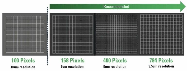
In addition to illumination, optical resolution is critical. With a 20 µm gap, enough pixels must be captured from edge to edge to achieve statistically valid and repeatable measurements. Each pixel represents a dataset of measurement values. Current resolutions of 5 µm and 3.5 µm per pixel are sufficient. For future requirements, optics with 1 µm resolution are already being prepared to ensure accurate capture even for denser structures. Resolution is always a trade-off between measurement quality and inspection speed. As pixel size decreases, the camera’s field of view also decreases, requiring more measurement fields to cover the entire substrate. The Meister D+ balances this with a 25-megapixel camera at 3.5 µm resolution, compensating for the smaller pixel size. If resolution is too coarse, individual pixels are more prone to fluctuation and may distort results. The more data points available, the more reliable and repeatable the measurement becomes. At 3.5 µm resolution, noise effects decrease dramatically, resulting in clean and dependable measurements.
Besides illumination and resolution, selecting the correct reference height is critical when measuring 20 µm gaps. Precise distance or height values require a reliable baseline, which can only be established when enough information about the substrate surface is available. In packaging, substrate quality is generally high. Nevertheless, surfaces can be challenging due to three-dimensional layer structures or semi-transparent layers. In such cases, local fiducials can be used directly on a silicon substrate or interposer. The fiducial surface offers excellent flatness, providing a stable foundation for precise reference heights. Even warpage can be compensated. Fiducial marks therefore provide a robust reference line.
What may seem like the future of high-density placement is already reality. The latest generation of mobile devices already uses this type of dense assembly in practice. And yes — it is being inspected during manufacturing. Our customers are already measuring these component-to-component distances in live production — with the Meister D+ platform at the package level and with the ZenStar platform at the wafer-level packaging stage.
Summary
The miniaturization of smartphone technology has reached the limits of wafer-level scaling, making advanced packaging the key to further integration and performance. Instead of fitting all functions into a single chip, heterogeneous packaging combines specialized chips in one housing, with System-in-Package as one important variant. This approach enables high-density assemblies with very small gaps between components, sometimes only 20 µm.
Such narrow distances create optical inspection challenges because the high aspect ratio forms deep gorges that are difficult to illuminate, and reflective die surfaces prevent conventional systems from capturing usable signals. To overcome this, the Meister D+ system employs a combination of multiple phase-shift projectors and coaxial illumination, enabling accurate detection of sidewalls, gaps, and reflective surfaces. High pixel resolutions further improve measurement quality, while stable reference heights are established through flat silicon or fiducial marks on substrates.
The results show that distances of 20–30 µm between SiP modules can already be measured reproducibly and reliably in production. What may seem like a future trend is, in fact, already established in industrial practice, with systems such as the Meister D+ and ZenStar platform ensuring precise inspection at both package and wafer level.
Curious about Koh Young? –
Productronica: Booth A2.377
Im Überblick
Fließtext std



