
Yes, there seems to be light at the end of the tunnel again. This cycle, as the others before, will surely come to an end. As Malcolm Penn of market research company Future Horizons expects, “This business will encounter recovery again in the forth quarter of 2002”. Because the wafer fabs are only used to a capacity of about 70% on a global scale at the moment, no company will invest in production capacity. That’s not today’s issue. But investment in capability, say in equipment that enables technologies or processes which could not efficiently provide before, is their issue. These can be, for example, ongoing developments in advanced packaging, in even smaller chip structures of 0,1 micron, and higher-resolution reproducing methods like deep-UV exposure. But in general, it seems that recession in this industry will hold itsgrip on us a bit longer than we have dreamed of for this year. Even in the year 2003, as in-dustry specialists expect, the recovery will basically not even reach the marvelous result of 2000.
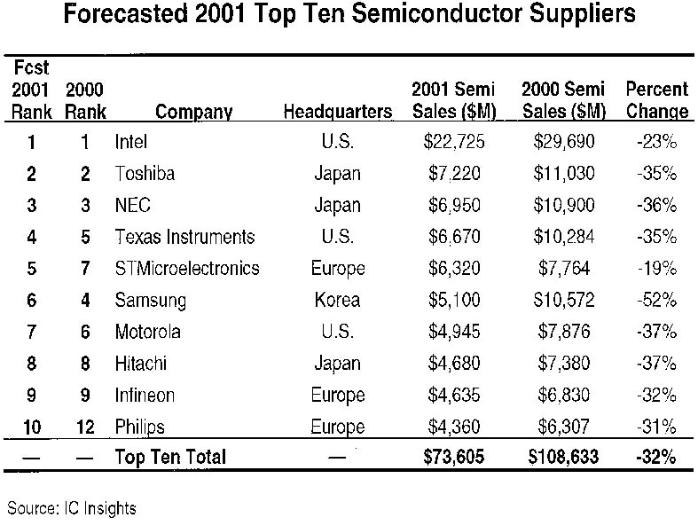
Just a short flash back to what happened last year. Otto Kosgalwies from ST Microelectronics describes the szenario: “2001 was the worst semiconductor market downturn ever, generated by the first US tech krach, amplified by the global US recession and the rise of uncertainties following the September 11th events”. And as Walter Roessger, president of Semi Europe, explains further, “The semiconductor revenues have dropped from $204bn down to 141bn (about minus 31%). And as one of the results of this drastic slump, the market volume for semiconductor capital equipment plunged from $48bn down to 31bn (-38%) in 2001. “We expect this year to recover slightly to 35bn.” But in the following two years the industry may perhaps see market volumes in high regions of about $40 to 50bn again. By the way: after the expected flying-high situation until 2004 – according to some predictions – with semiconductor revenues in the zenith of $238bn, the market will again switch over to the next downturn cycle. According to Semi, the total European semiconductor consumption lies on the average at 22% of the global figure, and the equipment shipments amount to about 13%.
Looking for the next upturn: where will most of the new wafer fabs be installed? Good question. It’s to a minor degree Europe, to a larger one North America and Japan, but the lion’s share will be erected in Asian countries, especially in China. There are some reasons for this: a large demand for semiconductors in mainland China, and the cost reduction in manufacturing of about 40%, compared to neighboring Taiwan (the other China). But make no mistake: labor cost is just one issue, the other is automation. Reportedly, a good example for this case is the Infineon memory manufacture in Europe, which is significantly more effective than its Asian competitors’, resulting in remarkably lower production costs. The other ongoing trend supporting a current demand for latest production equipment is the transition to 300mm silicon wafers. Here, very big investments in R&D, engineering of processes and machines alike and their carefully provided ramping-up, are necessary. The industry in this case plays the co-operation game to balance the load on different shoulders.
There is a whole range of events grouped around this focal trade show in mid April. These are about 30 key business meetings, sessions and conferences for all kinds of subjects associated with semiconductor and micro-electromechanical systems (MEMS) manufacturing, standards, technologies and fab management issues. Semi, currently consisting of more than 2500 members worldwide, has put a lot of efforts on this program. The industry organization takes its educational task very seriously and is eager to provide valuable programs, Europe executive Roessger didn’t get tired of underlining. (For detailed information with all information on the different occasions, please check Semi’s web site, mentioned at the article´s end.) The number of visitors expected this year would be in the range of 12,000. About 800 booths in 4 halls will be used to show products, services and other portfolio items. However, the shaky business climate and the mood of its actors is still widely influenced by the pressing question: how will the US economy, and in exchange Europe’s, develop? This circuit influences the semiconductor consumption and equipment business to a big extent, andin turn the global materialand equipment industries, too. Gerhard B.Wolski



