
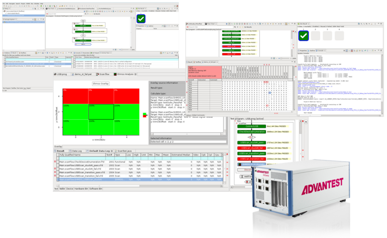
SiConic Link connects to standard evaluation boards through functional interfaces like USB, PCIe, control interfaces, and GPIOs. This enables test engineers to rapidly validate and debug design verification (DV) and design for test (DFT) content in SiConic’s unified environment on the bench.
Building on the V93000 test system’s leadership in scan over USB or PCIe, the solution’s unified environment brings native DV test content to test engineering without the error-prone and lengthy conversion and debug cycles typical for bring-up of advanced functional tests on ATE. Required for high-quality coverage in verification and test, functional testing enables a productivity boost for the bench collaboration of DV, DFT and test engineering.
Integrating seamlessly with SiConic Link hardware and the SmarTest 8 software platform, the solution provides users with comprehensive access to functional HSIO links for enhanced throughput and rich trace capabilities during test execution. By enabling smoother handoffs between silicon validation (SV), DV and TE teams, SiConic TE fosters tighter cross-domain collaboration.
Through its unified test environment and shared ecosystem, SiConic TE improves the correlation between bench, ATE and SLT systems. The tool’s optimized engineering resources allow bring-up and debug to be offloaded from ATE to the bench, freeing up valuable tester capacity and enabling more effective scaling. In addition, tight integration with leading EDA partners enables cross-functional collaboration with DV and DFT teams, improving test content development and speeding first-silicon success.
“[We are] expanding the SiConic vision to empower test engineers in a unified environment on the bench,” commented Juergen Serrer, chief technology officer and executive vice president at the company. “By moving bring-up and validation to scalable bench environments—and keeping DV, DFT, SV, and TE aligned through a scalable ecosystem—we’re helping customers validate faster, collaborate smarter, and maximize their engineering resources.”
Advantest developed SiConic TE in close collaboration with leading customers and EDA partners to ensure seamless integration into existing design and validation flows.
“Siemens EDA and Advantest have a long history of joint development on many DFT technologies, including Tessent Streaming Scan Network (SSN) and IJTAG,” stated Ankur Gupta, senior vice president and general manager, Digital Design Creation Platform, Siemens EDA, Siemens Digital Industries Software. “Collaborating on Advantest SiConic and Tessent In-System Test strengthens this long-running collaboration and helps to provide our users with time-to-market improvements and higher productivity.”
“As the scale and complexity of chips continue to increase, new verification approaches are needed to shift verification cycles earlier and deliver silicon with higher quality,” said Tom De Schutter, senior vice president of product management at Synopsys.



