Dr Kwangil Koh, Koh Young Technology
The basic science and techniques of automated optical inspection (AOI) of assembled circuit boards has not changed appreciably in recent times. Indeed, although many variations in equipment features and attributes exist among the different manufacturers – in terms of megapixel ratings, speed, and image processing – around the world, the basic operation of all systems is essentially the same in that two-dimensional (2D) imaging is the basis for the system’s analysis and determination of defects.
The topography and complexity of printed circuit assemblies has changed, as have manufacturing materials. Boards are more densely and compactly populated; components are smaller; with the advent of lead-free soldering, solder joints look different from their Pb-bearing counterparts of a decade ago and are subject to more problems and defects based on wetting, surface appearance, and the individual characteristics of the solder alloys. Acceptability standards, including IPC 610, have therefore also changed.
These and other issues have created problems for AOI in that the number of ‘escapes’ or undetected defects has risen. This has created real downstream problems and negatively affected the field reliability of products. In response, engineers have pushed their machines ever harder in the direction of more sensitive detection for the purpose of preventing escapes; but this has only resulted in an increasing number of false calls, which are also problematic and create manufacturing bottlenecks, slowing down production. Thus, false calls are almost as problematical as escapes. The root of the problem is the essential weakness of 2D imaging. Without sufficient visual data, the machine cannot make accurate calls, and begins making mistakes because it is being asked to do a more difficult task with insufficient tools. The answer is to provide better data.
Optimizing a manufacturing process for highest yields first requires that all soldering defects must be found by the AOI machine. For AOI, the number of defects found is not the problem; the number not found is. Defects found become someone else’s problem – the stencil printing process, pick and place, board solderability, or DFM – but they can then be addressed and solved at the appropriate step in the process. The defects that get by the AOI machine are the source of ongoing process headaches and compromised product reliability.
A technology has been developed that constitutes a radical departure from existing AOI vision technology in that it measures the vertical or Z-axis height of features being inspected in addition to the typical X-Y 2D image plane, and combines both. This added Z-dimension measurement solves many of the vulnerabilities of 2D AOI and makes it possible, finally, to detect all soldering defects on an assembly to prevent 100% of escapes. Real 3D measurement of solder joints was not possible until recently. The problems associated with 3D measurement had to be overcome, such as shadowing problems, measuring range, and soldered PCB warp and distortion. Any light measuring system is confronted with specular, reference plane shadow and directional problems which must be solved before one has a useful operating system.
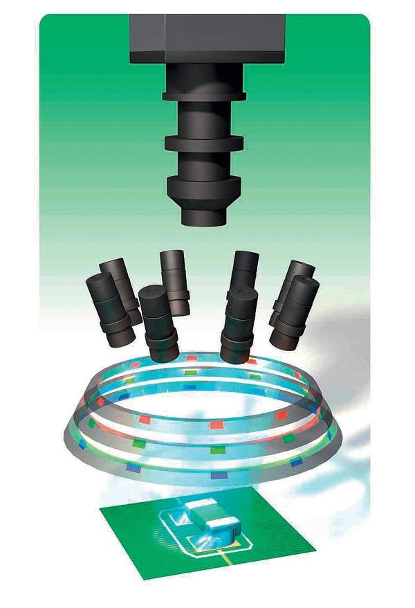
The AOI imaging head employs a series of eight white projection lights mounted in a circular configuration to pick up visual data from all sides and the top of the device or feature. It also contains multiple circular rows of LED illuminators positioned at different heights and angles to the part, each ring firing in succession in different colors, or wavelengths. The camera observes the varying wavelengths and angle of projection of each wavelength onto the part and thus can construct accurate 3D images and measure the height of the component or feature. This configuration allows for completely shadow-free imaging as well as precise position, shape, and height measurement of the feature under inspection.
The 3D image provides much more information to the machine to judge component position and the acceptability of the solder fillet. By comparing the measured values of the soldering fillet with IPC 610, the machine is able to make a clear ‘Go – No Go’ decision for, for example, solder joint inspection. This means that the evaluation criteria can be handled by an operator, who doesn’t need to judge if the solder joint is acceptable or not. The use of a globally-accepted standard (IPC 610) simplifies and speeds programming but also makes the identification of defects (and consensus) universal. CAD data provides the component/location guidelines and comparison against IPC 610 effectively closes the loop in flagging defects in coplanarity, polarity, lifted leads, tombstoning and others. In addition to nearly completely eliminating false calls and escapes, programming or teaching defects are also avoided.
The ability of the AOI machine to detect a missing component (such as a small chip capacitor) is critical. 2D AOI systems determine whether or not a component is missing by the shape of the fillet and template matching. Template matching is a comparison technology that compares what should be seen with what is actually seen, and requires considerable data interpretation for the machine to decide if there really is a ‘match’. For example, a round fillet might indicate that half of the fillet is not covered or hidden by an end termination; thus the component is missing. However, small fillet sizes or rectangular fillets may trigger the system to incorrectly flag a missing component, where one is not missing at all. This is a vulnerability of 2D AOI, whereas 3D AOI will use full profilometric component shape measurement technology rather than fillet shape to determine whether or not a component is missing. There is no possibility of error with 3D inspection; thus a common source of false calls is eliminated.
2D AOI has a weakness in that it cannot always determine the boundaries of solder and wetted component leads. This may result in undetected bridging if the body of the component interferes with the image or boundaries of the bridge; either a false call or escape may result, depending on what the 2D AOI system ‘thinks’ it sees. 3D sensing shows the profile and height of individual leads, and the gaps between them, showing positively whether or not bridging has occurred, thus preventing an incorrect determination by the machine.
The ability of a dark component to blend in with the board surface in 2D grayscale AOI is of no benefit to the engineer whose AOI system needs to find skewed or mis-located small components. The actual misalignment may not be detected; however with the ability to detect component height and shape with 3D sensing, the location of a component is precisely and immediately known to the system and can be flagged if it has been misplaced. Z-axis sensing removes the vulnerability to color that is a problem with 2D AOI.
Certain types of components such as the SOT 23 can be placed upside-down, and 2D AOI traditionally has a hard time detecting that flip. Again, the difficulty for the machine is distinguishing the difference between the soldered pads and the tinned leads. The leads will not be in contact with the pads at all but viewed from directly above, with the soldered pad as background, the AOI machine cannot make a distinction between them or sense that they are not connected. 3D imaging however will immediately show that the position of the leads is too high, and that they are not connected at all to the pads at a lower level. The ability of the machine to ‘see’ this effectively eliminates this potential escape.
The same problem arises when the SOT is skewed or mis-located; it is dark, and its leads are not easy to distinguish from the fillet. Failure to detect a component shift is the result, because the component’s location cannot be determined. The solution is to detect component body shape using 3D imaging and then to compare it with the data showing where it ought to be.
2D inspection is like viewing a landscape from an altitude using only one eye. There is no depth perception; the height of objects cannot be determined without some foreknowledge on the part of the person making the observation. But since the peaked roofs of houses in a neighborhood, for example, all look the same from the sky, there is no way to tell, without a side view or element of depth perception, whether or not all the buildings are single story or multi-stories in height. The same is true for lifted leads, and lifted components. 2D AOI cannot determine whether or not these components are at the proper height for an object connected to the PCB. 3D sensing can immediately show if one lead, or one side of a component is higher than the others, i.e., not planar to the surface of the board. This is especially effective when detecting lifted leads. 2D AOI uses fillet shape to determine the status of leads, and with very small fillets, it is inadequate. 3D AOI also allows far more accurate shape measurement of fillets, which may be critical in many cases.
Small passive components nestled between two larger active devices, e.g., two BGAs, present a problem for 2D AOI in that shadowing may make it impossible for the machine to ‘see’ the chip and determine whether or not it is there, or properly positioned, etc. Using 3D AOI will help, but again the component must be ‘seen’, and the chances are better that it will using a circle of eight light projections. Not all projections will be able to see it, but enough will that a z-axis measurement can be made of the site to determine the presence and shape of the tiny component for an effective result.
Manufacturing engineers using AOI are not concerned about the defects that their machines find, but rather the escapes that the machine does not catch. The consequences of then trying to push their machines beyond their limitations – which are imposed by the inadequacies of 2D imaging data – are false calls. The problem becomes worse as components become ever-smaller on tightly-packed assemblies. The solution is improved data – 3D imaging and measurement – by adding another dimension (Z-axis) to the 2D information already used by the AOI system. 3D AOI effectively negates all of the shortcomings of traditional 2D AOI and eliminates virtually all possibility of escapes while also preventing false calls due to shadowing and specular problems that have long been the primary vulnerabilities of 2D AOI.
eppe440
Um ja nichts zu übersehen werden AOI-Systeme über ihre technischen Möglichkeiten hinaus scharf eingestellt und geben deshalb häufig falschen Alarm. 3D AOI macht mit dieser zeitaufwändigen Arbeitsweise Schluss.
Les systèmes AOI sont souvent réglés avec une précision qui excède leurs possibilités techniques, d’où un risque de fausses alarmes. Grâce aux systèmes AOI 3D, cette manière de procéder appartient au passé.