
Zum Inhalt springen
EPP Europe
  • News
  • Products
  • Applications
  • Technology
  • Semiconductor
  • Inspection
  • Company News
  • Events
EPP Europe
  • Technology
  • Inspection (AOI/AXI)
  • Semiconductor Packaging
  • Company News
  • Products
  • Trade Shows & Events
    EPP Europe Newsletter
    The most important electronics-manufacturing news delivered to your inbox.

    Info

    • Impressum
    • Datenschutz
    • Barrierefreiheit
    • Datenschutzeinstellungen

    Kontakt zur Redaktion

    EPP EuropeKonradin Mediengruppe
    Ernst-Mey-Str. 8, 70771 Leinfelden-Echterdingen

    E-Mail: redaktion@konradin.de
    Folgen Sie uns
    EPP Europe
    © 2026 EPP Europe
    Startseite/Electronica-2022/Artikel
    CyberOptics to feature yield-improving auto-teaching systems
    Bildquelle nicht angegeben
    Electronica-2022

    CyberOptics to feature yield-improving auto-teaching systems

    CyberOptics Corporation, a leading global developer and manufacturer of high-precision 3D sensing technology solutions, will exhibit at Semicon Europa
    Veröffentlicht
    09. Oktober 2022
    Lesezeit
    1 Minute
    Rubrik
    Electronica-2022

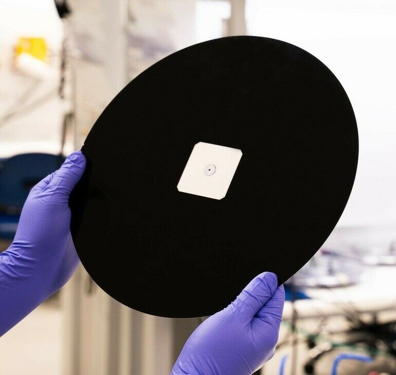
    ATS2 and ATSR are multi camera sensors used with CyberSpectrum software to teach accurate wafer and reticle hand-off calibration for proper alignment and set-up of semiconductor tools. The sensors „see“ inside to capture three dimensional off-set data (x, y and z) in real-time to quickly teach wafer and reticle transfer positions – all without opening the tools. Process and equipment engineers can conduct repeatable and reproducible setups and maintenance checks, speed trouble-shooting and eliminate technician-to-technician variation.

    The company will also feature the In-Line Particle Sensor (IPS) with the software that detects particles in gas and vacuum lines 24/7 down to 0.1µm. The sensor is particularly relevant for EUVL tools to monitor particles in-line. The device is an extension of the industry-leading Airborne Particle Sensor (APS/APSRQ) technology that is documented by fabs as the Best-Known Method (BKM).

    WaferSense and ReticleSense sensors are widely used for various applications including leveling, vibration, gapping, relative humidity, resistance and airborne particles. Semiconductor fabs worldwide rely on these real-time measurement sensors to improve yields, processes and tool uptime.

    Semicon Europa, Stand C1101

    www.cyberoptics.com

    Mehr aus Electronica-2022

    Weitere aktuelle Artikel aus der Rubrik Electronica-2022.

    Alle Electronica-2022-Artikel
    GÖPEL electronic to debut Multi Line AXI platform and updated AOI and boundary scan portfolio at electronica 2026Foto: Laurens van der Drift / Unsplash
    Electronica-2022

    GÖPEL electronic to debut Multi Line AXI platform and updated AOI and boundary scan portfolio at electronica 2026

    13. September 2026

    GÖPEL electronic is set to introduce the Multi Line AXI, an entirely new X-ray inspection platform, at electronica 2026, alongside updates to its AOI and boundary scan product lines. The announcement positions the…

    ← Zurück zu Electronica-2022Zur Startseite