
Zum Inhalt springen
EPP Europe
  • News
  • Products
  • Applications
  • Technology
  • Semiconductor
  • Inspection
  • Company News
  • Events
EPP Europe
  • Technology
  • Inspection (AOI/AXI)
  • Semiconductor Packaging
  • Company News
  • Products
  • Trade Shows & Events
    EPP Europe Newsletter
    The most important electronics-manufacturing news delivered to your inbox.

    Info

    • Impressum
    • Datenschutz
    • Barrierefreiheit
    • Datenschutzeinstellungen

    Kontakt zur Redaktion

    EPP EuropeKonradin Mediengruppe
    Ernst-Mey-Str. 8, 70771 Leinfelden-Echterdingen

    E-Mail: redaktion@konradin.de
    Folgen Sie uns
    EPP Europe
    © 2026 EPP Europe
    Startseite/Semiconductor-packaging/Artikel
    CyberOptics Features New Dual-Mode MRS Sensor at Smart SMT & PCB Assembly in Korea
    Bildquelle nicht angegeben
    Semiconductor-packaging

    CyberOptics Features New Dual-Mode MRS Sensor at Smart SMT & PCB Assembly in Korea

    CyberOptics Corporation (NASDAQ: CYBE), a leading global developer and manufacturer of high-precision 3D sensing technology solutions will feature the
    Veröffentlicht
    08. April 2022
    Lesezeit
    2 Minuten
    Rubrik
    Semiconductor-packaging

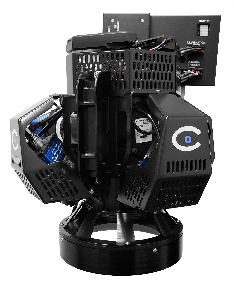
    The SE3000 SPI System incorporates the new Dual-Mode MRS sensor for superior performance and maximum flexibility for dedicated solder paste inspection applications, with one mode for high-speed, and another mode for high resolution. The new sensor is an extension of the proprietary sensor portfolio that provides industry-leading performance in semiconductor and SMT markets. Customers value the high accuracy, repeatability and reproducibility of the SE3000 that is ideal for detecting insufficient or excessive paste, height, area and other SPI applications.

    “For dedicated SPI applications, we have integrated our new Dual-Mode MRS sensor into the SE3000 system to provide superior performance and flexibility,” said Dr. Subodh Kulkarni, President and CEO, CyberOptics. “With this addition to our portfolio of systems, customers have another option that can significantly improve their yields, processes and productivity.”

    The SQ3000+ Multi-Function system powered by MRS for inspection and metrology is an extension of the multi-award-winning SQ3000 platform deemed best-in-class, that not only conducts AOI and SPI, but uniquely delivers in-line, full coordinate measurement (CMM) data in seconds, not hours.

    CyberOptics’ unique MRS sensor architecture simultaneously captures and transmits multiple images in parallel while proprietary 3D fusing algorithms merge the images together, delivering metrology grade accuracy at production speed. Effective suppression of multiple reflections from shiny components and surfaces is critical for highly accurate inspection and metrology, making it an ideal technology solution for a wide range of applications with high quality requirements.


    Mehr aus Semiconductor-packaging

    Weitere aktuelle Artikel aus der Rubrik Semiconductor-packaging.

    Alle Semiconductor-packaging-Artikel
    Nanoscribe Expands Photoresin Portfolio for Micro-Optics Fabrication via Two-Photon PolymerizationFoto: Brecht Corbeel / Unsplash
    Semiconductor-packaging

    Nanoscribe Expands Photoresin Portfolio for Micro-Optics Fabrication via Two-Photon Polymerization

    11. November 2026

    Nanoscribe has detailed its range of photoresins engineered for Two-Photon Polymerization (2PP) and Two-Photon Grayscale Lithography (2GL), targeting high-precision micro-optics manufacturing on silicon, glass, and…

    Canon Launches FPA-6400ES6a KrF Lithography System with 400 Wafers-per-Hour ThroughputFoto: Canon Europe (semicon)
    Semiconductor-packaging

    Canon Launches FPA-6400ES6a KrF Lithography System with 400 Wafers-per-Hour Throughput

    10. November 2026

    Canon has announced the FPA-6400ES6a KrF scanner for semiconductor lithography, combining a throughput of 400 wafers per hour with industry-leading overlay accuracy of 4.0 nm and the ability to handle wafer warpage of…

    Fabmatics absorbs SCI business activities under unified brandFoto: Ludovico Ceroseis / Unsplash
    Semiconductor-packaging

    Fabmatics absorbs SCI business activities under unified brand

    6. November 2026

    Fabmatics has integrated the business activities of SCI under the Fabmatics brand, consolidating the acquired expertise within its semiconductor automation portfolio.

    Entegris and Kioxia Expand Partnership on Materials Innovation for Next-Gen 3D Flash MemoryFoto: Louis Reed / Unsplash
    Semiconductor-packaging

    Entegris and Kioxia Expand Partnership on Materials Innovation for Next-Gen 3D Flash Memory

    6. November 2026

    Entegris and Kioxia are deepening their strategic partnership to co-develop materials and process technologies for future BiCS FLASH 3D NAND architectures, using AI, digital-twin modelling and experimental validation at…

    ← Zurück zu Semiconductor-packagingZur Startseite

