
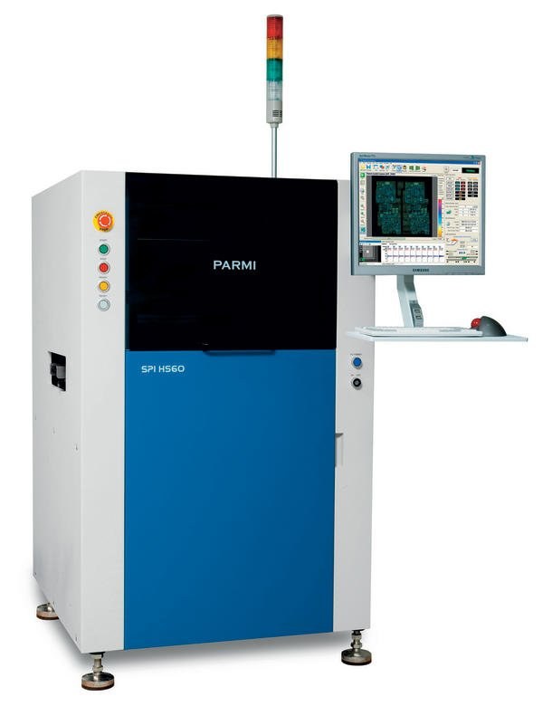
Detection of incorrect solder paste deposition due to paste variance, stencil cleanliness and poor machine condition is significantly less expensive to achieve than AOI systems further down the line, and the rework costs at the front end are significantly lower. The development of electronic, IT and communication technologies has required that the products be compact, light, high-end and high speed, causing components on the PCBs to become smaller and smaller such as BGA, CSP and 01005 etc., which cannot be detected by the human eye. Therefore, inspection of the printing condition is becoming essential in the SMT production line. Competition on the quality and price of products has been significantly increased, so 6 sigma has become the core of the business. This leads process inspection technology to be essential which results in requirements upon the inspection process for every SMT production line.
Solder paste related defects continue to top many manufacturers’ lists as the process becomes responsible for the greatest percentage of end of line defects. After solder reflow, defects can be much more costly to repair, and risk of damaging the board or the components during the rework process increases. A more effective strategy would be to improve first pass yields and prevent these defects from occurring in the first place. The introduction and usage of smaller component packaging in electronic assemblies rapidly increases those results which raise the importance of solder paste inspection. Low quality of solder joints will cause high servicing cost and complaints from customers in the long run. Solder paste inspection can play an important role in eliminating defects as a source of problems and helping clarify the remaining causes of problems in the process.
The solder paste deposition process continues to be the leading source of end of line defects in the SMT assembly process. Solder paste printing (even though the printing equipment and process has become much more reliable over the past 10 years) is still a complex process where many process variables, materials, environmental influences (temperature and humidity), and human factors, meet. It is consistently reported that this process step continues to be responsible for the greatest number of end of line defects. Changing the process to accommodate smaller packages, new stencil designs and paste formulations will make it more difficult to maintain high yields.
Inspection systems have also been developed as the industries grow, and 2 D inspection systems showed their limitations on accurately inspecting the printing process. Camera-based systems of 2 D SPI are only capable of measuring area coverage and alignment. It is sensitive to color and contrast changes, but more importantly lack of height and volume information was the main limitation of 2 D SPI. Area alone is not a reliable indicator of the correct amount of paste present. 3 D SPI is capable of providing all volume, height and area measurements and it adds benefits of being insensitive to color and contrast changes because it is much easier to configurate (figure 2 and 3). Solder paste volume information is a good predictor of finished board quality. Furthermore, solder paste volume is a key variable to deciding the quality of solder joints. Insufficient solder paste volume may pass ICT tests but it can cause the potential defects after shipment as an end product. Characteristic of solder paste is that its shape can be reformed by melting after reflow. Therefore, solder paste volume is required to be analyzed to predict the result after reflow. This makes 3D measurement a requirement for SPI machines, unlike AOI systems.
The cost to repair a defect such as solder bridges (figure 4) increases substantially as it moves undetected through the assembly process. Rework is expected to be more difficult and expensive because the device and labor costs may be high. When these problems are found before the next process step, the cost to correct the problem can often be reduced by 10 times or more. A more effective test strategy would be to improve first pass yields and prevent these defects from occurring in the first place by inspecting the paste immediately after print. SPI system will help to remove defects at the stage that maximizes saving rework cost at the SMT assembly line. One of the main roles of SPI system is increasing First Pass Yield (FPY) by reducing the number of defects, improving the quality of production process and reducing the time for production line to be stable after line setup or job change. It also prevents the potential defects from solder joints which will result in higher in reliability of the products for the customer.
No matter what types of light source (laser, sinusoidal strips for PSP) are projected on panels, the intensity of image through camera imaging optics will be very much dependent on colors and materials variation (naked pad , silk, solder paste, solder register on pads, solder register on epoxy) and surface treatment method etc. of the panel. The intensity could be varied for hundreds of times, and management of these problems affect to the performance of SPI systems directly. The Moire measuring principle minutely moves a sinusoidal strip 3 or 4 times and develops a height by examining the imaged brightness change at a certain point. And this method demands high linearity of the camera detector. However, there is no camera with high linearity and large bandwidth, so it fails to collect data on very dark areas and very bright areas, causing detector saturation.
Parmi’s measuring principle, optical triangulation, which extracts the centroid of the laser beam, has no problem concerning brightness of light entering to the camera (figure 5). Laser is immune to changes in external environment such as outdoor light and color of objects, and hardware design of laser SPI systems is comparably simple and therefore is a robust structure to be used for a long time with no deformation or troubles. Inspection speed can be improved constantly by improving the processing speed of the camera so these SPI systems have the fastest inspection speed in the market. The included software contains multiple tools for 3D analysis and statistical evaluation (figure 6).
Three SPI models (offline, bench-top and in-line) are offered to meet diverse demands from customers, and are proud of being the best machines in the worldwide market. The company uses a very compact and high speed laser system which gives high accuracy and repeatability. Parmi also uses gantry mechanism so only one stage conveyor system is used which makes the system simple, using a very few number of parts, which leads to easy maintenance. Moreover, x-axis is used to scan and is driven by a linear motor, and the large model uses dual drive on y-axis due to gantry type positional accuracy. Gantry type holds the PCB during the inspection process so the vibration effect is small, and the back up pin is easy to apply which compensates directly for warpage. Development and production of all products are done by 100 % pure self-developed technology and software so it is possible to cope flexibly with improvement on any functions or other customer’s requests by active upgrades on the technology and software.
EPP Europe 442
Die Lotpasteninspektion ermöglicht die Bewertung der Baugruppe vor dem Lötprozess. So können viele Folgekosten infolge von Ausmusterungen, Nacharbeit und Beschwerden vermieden werden, da die meisten dieser Fehler durch schlechten Lotpastendruck hervorgerufen werden. Die Systeme analysieren die Baugruppen-Oberfläche dreidimensional mittels Lasertriangulation, eine Technologie, die bekannt ist für die hohe Präzision und Geschwindigkeit des Messwerterfassungssystems. Der Anwender erhält umfassende Informationen über Bereich, Höhe, Lage und Umfang der Lotpaste in der Baugruppe.
L’inspection de la pâte à braser permet d’analyser les composants avant le brasage. Il est ainsi possible d’éviter de nombreux frais découlant de mises au rebut, de post-usinages et de plaintes, étant donné que la plupart de ces problèmes sont dus à une pression incorrecte de la pâte à braser. Les systèmes analysent la surface des composants en trois dimensions à l’aide d’une triangulation laser, une technologie connue pour la précision et la vitesse élevées du système d’acquisition des valeurs mesurées. L’utilisateur reçoit des informations complètes sur l’étendue, l’épaisseur, la position et la quantité de pâte à braser dans le composant.
L’ispezione della pasta per saldare permette la valutazione del componente prima del processo di saldatura. In questo modo è possibile evitare molti costi derivanti da ritiro, ritocco e reclami, poiché la maggior parte di questi errori derivano da cattiva pressione della pasta per saldare. I sistemi analizzano la superficie dei componenti in modo tridimensionale mediante triangolazione laser, una tecnologia nota per l’alta precisione e velocità del sistema di raccolta dei valori misurati. L’utilizzatore ottiene informazioni esaurienti circa zona, altezza, posizione e perimetro della pasta per saldare nel componente.



