
Zum Inhalt springen
EPP Europe
  • News
  • Products
  • Applications
  • Technology
  • Semiconductor
  • Inspection
  • Company News
  • Events
EPP Europe
  • Technology
  • Inspection (AOI/AXI)
  • Semiconductor Packaging
  • Company News
  • Products
  • Trade Shows & Events
    EPP Europe Newsletter
    The most important electronics-manufacturing news delivered to your inbox.

    Info

    • Impressum
    • Datenschutz
    • Barrierefreiheit
    • Datenschutzeinstellungen

    Kontakt zur Redaktion

    EPP EuropeKonradin Mediengruppe
    Ernst-Mey-Str. 8, 70771 Leinfelden-Echterdingen

    E-Mail: redaktion@konradin.de
    Folgen Sie uns
    EPP Europe
    © 2026 EPP Europe
    Startseite/Semiconductor-packaging/Artikel
    Christian Koenen: High performance printing processes for flux printing application
    Bildquelle nicht angegeben
    Semiconductor-packaging

    Christian Koenen: High performance printing processes for flux printing application

    Christian Koenen GmbH shares their expertise on printing processes for the semiconductor packaging industry.
    Veröffentlicht
    19. Juli 2022
    Lesezeit
    2 Minuten
    Rubrik
    Semiconductor-packaging

    To be able to migrate from precision placement of SMD to semiconductor packaging, a knowledge transfer in several areas of the supply chain is going to take place. Christian Koenen GmbH believes that soon many SMD manufacturer will also produce components and be able to manufacture mid-size or even high quantity batches.

    With this newsletter, the company will support SMD and semiconductor manufacturing with information about very efficient, high performance print processes for semiconductor packaging. In the coming months, the company will share experience specifically about the following topics:

    Semiconductor backend processes

    • Bumping
    • Balling
    • Flux printing
    • Chip assembly
    • Chip stack assembly
    • Pre-bowed Chip assembly
    • Copper Pillar chip assembly
    • Chip moulding and filling
    • Conventional LED assembly
    • Min-LED assembly

    Flux printing application process

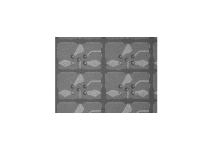
    One of the reasons for flux to be printed on the surface of PCB’s or substrates is to break off all oxides. It also cleans the contact area to allow the solder to get into a metallic connection of the contact pads. Flux printing in support of solder interconnection is needed for many assembly processes, but especially for flip chip assembly and balling processes.

    Flux applications are done in different ways such as dispensing, dipping or printing.
    In regard to productivity and process speed, very often a dipping process takes ~1/3 of a second and a dispenser process ~ 1 sec. per dot. Alternatively, the print process takes 30 sec. but covering the whole area of the substrate in one print stroke.

    In cases where more than 30 flux dots or more than 100 dice needed to be placed, flux printing is not only more economic, but also often more repeatable. If economics and process control have highest priority, then flux printing is in many cases the best choice.

    At Christian Koenen GmbH, they have extensive process knowledge to design and manufacture those specialized flux printing stencils. The company is also able to test and trial those kinds of prints in their Application Lab with extensive analysis and checks to prepare and prove the individual processes for the customer. State of the art process equipment and measurement methodology is available and used to perform these prints.


    Mehr aus Semiconductor-packaging

    Weitere aktuelle Artikel aus der Rubrik Semiconductor-packaging.

    Alle Semiconductor-packaging-Artikel
    Nanoscribe Expands Photoresin Portfolio for Micro-Optics Fabrication via Two-Photon PolymerizationFoto: Brecht Corbeel / Unsplash
    Semiconductor-packaging

    Nanoscribe Expands Photoresin Portfolio for Micro-Optics Fabrication via Two-Photon Polymerization

    11. November 2026

    Nanoscribe has detailed its range of photoresins engineered for Two-Photon Polymerization (2PP) and Two-Photon Grayscale Lithography (2GL), targeting high-precision micro-optics manufacturing on silicon, glass, and…

    Canon Launches FPA-6400ES6a KrF Lithography System with 400 Wafers-per-Hour ThroughputFoto: Canon Europe (semicon)
    Semiconductor-packaging

    Canon Launches FPA-6400ES6a KrF Lithography System with 400 Wafers-per-Hour Throughput

    10. November 2026

    Canon has announced the FPA-6400ES6a KrF scanner for semiconductor lithography, combining a throughput of 400 wafers per hour with industry-leading overlay accuracy of 4.0 nm and the ability to handle wafer warpage of…

    Fabmatics absorbs SCI business activities under unified brandFoto: Ludovico Ceroseis / Unsplash
    Semiconductor-packaging

    Fabmatics absorbs SCI business activities under unified brand

    6. November 2026

    Fabmatics has integrated the business activities of SCI under the Fabmatics brand, consolidating the acquired expertise within its semiconductor automation portfolio.

    Entegris and Kioxia Expand Partnership on Materials Innovation for Next-Gen 3D Flash MemoryFoto: Louis Reed / Unsplash
    Semiconductor-packaging

    Entegris and Kioxia Expand Partnership on Materials Innovation for Next-Gen 3D Flash Memory

    6. November 2026

    Entegris and Kioxia are deepening their strategic partnership to co-develop materials and process technologies for future BiCS FLASH 3D NAND architectures, using AI, digital-twin modelling and experimental validation at…

    ← Zurück zu Semiconductor-packagingZur Startseite

