
Zum Inhalt springen
EPP Europe
  • News
  • Products
  • Applications
  • Technology
  • Semiconductor
  • Inspection
  • Company News
  • Events
EPP Europe
  • Technology
  • Inspection (AOI/AXI)
  • Semiconductor Packaging
  • Company News
  • Products
  • Trade Shows & Events
    EPP Europe Newsletter
    The most important electronics-manufacturing news delivered to your inbox.

    Info

    • Impressum
    • Datenschutz
    • Barrierefreiheit
    • Datenschutzeinstellungen

    Kontakt zur Redaktion

    EPP EuropeKonradin Mediengruppe
    Ernst-Mey-Str. 8, 70771 Leinfelden-Echterdingen

    E-Mail: redaktion@konradin.de
    Folgen Sie uns
    EPP Europe
    © 2026 EPP Europe
    Startseite/Semiconductor-packaging/Artikel
    Bosch opens semiconductor test centre in Malaysia
    Bildquelle nicht angegeben
    Semiconductor-packaging

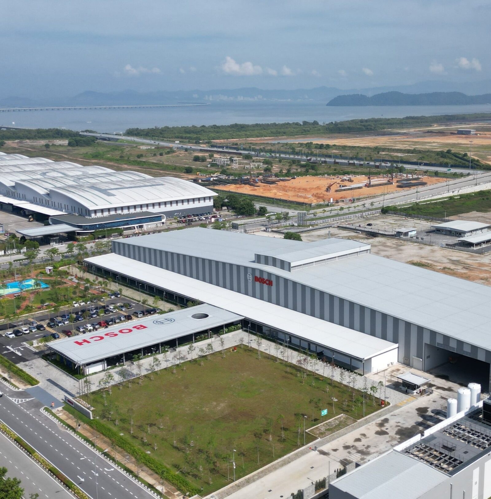
    Bosch opens semiconductor test centre in Malaysia

    Global supplier of technology and services Bosch has opened an advanced semiconductor backend site in Penang, Malaysia for the testing of its automotive
    Veröffentlicht
    04. August 2023
    Lesezeit
    2 Minuten
    Rubrik
    Semiconductor-packaging

    The company plans to invest around EUR 350 million in the site by the mid-2030s, and generate around 400 jobs. The facility currently spans 18,000 sqm, including clean rooms, office space, and laboratories for quality assurance and manufacturing. The total land area comprises around 100,000 sqm.

    “The Penang backend site is a key component in our growth strategy in the mobility sector as we respond to the increased demand for semiconductors,” said Klaus Maeder, Member of the Bosch Mobility Sector Board Responsible for Operations. “We chose to invest in Penang for its high level of semiconductor knowledge and skilled workforce. The proximity to business partners and customers is another advantage, as it will shorten delivery times and distances for the chips.”

    “With our new semiconductor test center in Penang, we are creating additional capacity within our worldwide manufacturing network to meet the continued high demand for chips and sensors,” said Dr. Stefan Hartung, chairman of the Bosch board of management. “Semiconductors are a decisive success factor for all Bosch business areas, and the expansion of this business is strategically very important.”

    “With a total of 4,200 associates and nearly RM400 million (86.2 million EUR) investments in Malaysia, as of December 31, 2022, Penang is home to the largest number of manufacturing facilities in a single country for Bosch in Southeast Asia,” the company said in a press release. “With the addition of an advanced backend site in Southeast Asia, the company is completing its internal process chain especially for the semiconductors manufactured in Dresden, Germany.”


    Mehr aus Semiconductor-packaging

    Weitere aktuelle Artikel aus der Rubrik Semiconductor-packaging.

    Alle Semiconductor-packaging-Artikel
    Kosmek Publishes Semiconductor Manufacturing Automation CatalogFoto: Kosmek (semicon)
    Semiconductor-packaging

    Kosmek Publishes Semiconductor Manufacturing Automation Catalog

    13. November 2026

    Kosmek has released an industrial automation catalog focused on semiconductor manufacturing, detailing pneumatic supports, robotic hand changers and locating components applicable across front-end and back-end…

    Nanoscribe Expands Photoresin Portfolio for Micro-Optics Fabrication via Two-Photon PolymerizationFoto: Brecht Corbeel / Unsplash
    Semiconductor-packaging

    Nanoscribe Expands Photoresin Portfolio for Micro-Optics Fabrication via Two-Photon Polymerization

    11. November 2026

    Nanoscribe has detailed its range of photoresins engineered for Two-Photon Polymerization (2PP) and Two-Photon Grayscale Lithography (2GL), targeting high-precision micro-optics manufacturing on silicon, glass, and…

    Canon Launches FPA-6400ES6a KrF Lithography System with 400 Wafers-per-Hour ThroughputFoto: Canon Europe (semicon)
    Semiconductor-packaging

    Canon Launches FPA-6400ES6a KrF Lithography System with 400 Wafers-per-Hour Throughput

    10. November 2026

    Canon has announced the FPA-6400ES6a KrF scanner for semiconductor lithography, combining a throughput of 400 wafers per hour with industry-leading overlay accuracy of 4.0 nm and the ability to handle wafer warpage of…

    Fabmatics absorbs SCI business activities under unified brandFoto: Ludovico Ceroseis / Unsplash
    Semiconductor-packaging

    Fabmatics absorbs SCI business activities under unified brand

    6. November 2026

    Fabmatics has integrated the business activities of SCI under the Fabmatics brand, consolidating the acquired expertise within its semiconductor automation portfolio.

    ← Zurück zu Semiconductor-packagingZur Startseite

